
Dektak XTL
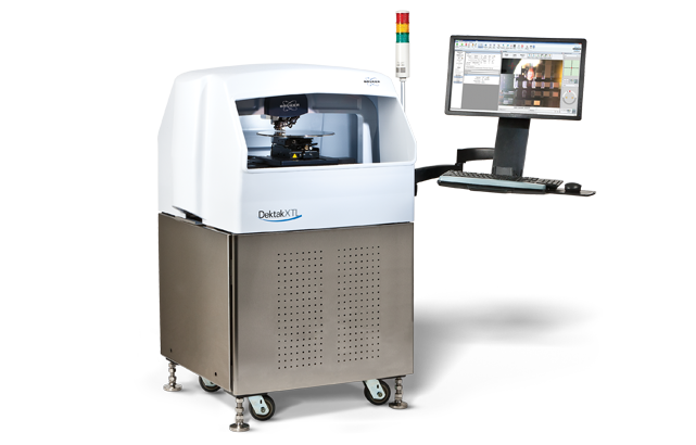
Dektak X
触針式プロファイリングシステムDektak XTLは、正確度、繰り返し性、再現性が極めて高く、幅広い用途に対応する計測システムです。350 mm x 350 mmまでのサンプルを搭載できるため、定評あるDektakシステムの性能を200 mmおよび300 mmウエハ製造にも活用できます。インターロックドアによる隔離機能を備えたDektak XTLは、要求の厳しい現在の生産環境に最適です。カメラ2台の構成により空間認識性能が上昇し、高度な自動化により製造スループットが向上します。
卓越した性能と使いやすさを兼ね備えたDektak XTLは、タッチパネル、太陽電池、フラットパネルディスプレイ、半導体分野の産業用薄膜形成モニタリングの研究およびQA/QCでの評価において、新たな標準装置となる製品です。
業界最高の自動化・分析ソフトウェア
ソフトウェアの拡張機能により、Dektak XTLは最も強力で最も使いやすいスタイラスプロファイラとなりました。このシステムは、Brukerの光学プロファイラ製品と完全に互換性のあるVision64ソフトウェアを使用しています。 Vision64ソフトウェアは、無数の測定サイト、3Dマッピングのほか、何百もの内蔵分析ツールで高度にカスタマイズされた特性評価を可能にします。
また、Vision Microformソフトウェアを使用して曲率半径などの形状を測定することもできます。オペレータのエラーを最小限に抑え、測定位置の精度を高めるためにパターン認識を使用します。データ収集と2Dおよび3D解析は、直感的な流れで1つのソフトウェアパッケージにまとめられています。各システムには、Windows 10 OSを搭載した別のPCにインストールできるVisionソフトウェアライセンスが付属しているので、データ分析とレポートをデスクで作成できます。

比類のないスタイラステクノロジー

Dektak XTLは、50年以上にわたる触針式スタイラスの開発実績と生産設備向けのアプリケーションのカスタマイズを基に設計されており、現在および将来の厳しい業界のロードマップに対応しています。300ミリの高精度エンコードされたXYステージングは、厳しいゲージR&R要件を満たすための信頼性の高いツールを提供します。高倍率デュアルビューカメラを搭載したDektakのデュアルカメラコントロールは、空間認識機能を強化。ライブビデオでのポイントアンドクリックによる位置決めにより、オペレータは迅速で簡単な測定セットアップと自動化プログラミングのために、サンプルを適切な位置に素早く配置することができます。システムの大きなインターロックドアは、サンプルのロード/アンロードのための安全で簡単なアクセスを提供します。
その他のハードウェア機能は以下の通りです。
- 業界をリードする性能を実現するシングルアーチアーキテクチャと防振構造内蔵
- クイックチェンジセルフアライメントスタイラス
- 高精度エンコードされたXYステージにより、より迅速な自動データ収集を実現
- ソフトタッチ技術と1mmの測定範囲を持つN-Liteの低力は、繊細で高垂直範囲のサンプルを測定するために同時に使用することができます。
Frequently Asked Questions
Dektak XTL is designed for large-format and production-oriented measurements. It combines a motorized, high-accuracy encoded 300 mm XY stage, continuous 360° theta positioning, an enclosed workstation, integrated vibration isolation, and automation capabilities for process development and QA/QC environments.
Dektak XTL accommodates wafers up to 300 mm and samples up to 350 mm × 350 mm, with a maximum sample thickness of 50 mm. This supports both large wafers and panel or other large-substrate applications.
Dektak XTL uses dual-camera viewing with top and high-magnification side views. Operators can easily navigate to points of interest, orient the sample, and define scan start and end positions directly from the live video.
The encoded 300 mm XY stage and continuous theta positioning support automated measurements at unlimited measurement sites. Operators can program fiducials and measurement sites, while pattern recognition can improve measurement-location accuracy and reduce operator-to-operator variability. Measurement results can also be automatically analyzed and logged to a database.
Common applications include semiconductor wafers, touch panels, flat-panel displays, solar coatings, printed circuit boards, and flexible electronics. Measurements include deposited-film and resist step height, etch-rate determination, CMP erosion and dishing, coating thickness, and printed circuit board bumps and step heights.
You can request a quote using our online form, or contact us directly.
More About Bruker's Dektak Stylus Profiler Systems
The sample is placed on a slider that slides over a highly polished flat glass block. The surface profile is measured by drawing the sample slider at constant speed underneath the stylus tip.
The vertical movement of the stylus tip is measured using LVDT (Linear Variable Differential Transformer) technology, which converts the stylus displacement into a highly precise and linear electrical signal.
Benchtop systems can accommodate small coupons up to full 8” wafers, while production models support large wafers and panels up to 12” size with encoded stages and multi‑site automation. The maximum sample height is 50 mm. Exact limits depend on the model, stage travel, and accessories.
For step height, typical vertical repeatability is on the order of a few angstroms to ~1 nm under controlled conditions, with sub‑nanometer repeatability possible on optimized setups and certified standards. Some key variables affecting accuracy and repeatability are tip condition/geometry, applied force, sample fixturing, vibration/thermal stability, and analysis procedures.
The standard stylus force of a Dektak stylus profiler ranges from 1 to 15 mg. For very delicate materials the force range can be extended downward to 0.03 mg (N-Lite force range).
The Dektak diamond stylus tips have a cono-spherical shape with radii ranging from 25 µm down to very sharp 50 nm. Often, Dektak stylus profilers are equipped with a stylus tip with 2 µm radius which is the recommended stylus radius for roughness measurements.
Sharper styli may be used if higher lateral resolution is required, while styli with greater radii may be useful on very sensitive surfaces.
Dektak styli are easily exchanged within a minute with the included stylus exchange tool. No tiny screwdrivers, Allen wrenches, or tweezers needed. No recalibration needed: Stylus exchange does not affect the calibration of the vertical scale, force scale or optical view.
Every Dektak stylus profiler supports recipe-based workflows for measurement and data analysis. In addition to measurement and automated analysis, Dektak recipes support the acquisition of sample information (e.g., wafer ID and part number), automatic saving of data files using template-generated filenames, and reporting of analysis results (e.g., step heights and roughness) to database tables.
Dektak stylus profilers with motorized XY-stage also allow to generate and run multi-site automation recipes, complete with wafer registration with alignment features (manual or by optical pattern recognition) and automated analysis and database reporting.
Selecting and Upgrading a Dektak Stylus Profiler
- The sub-nm vertical resolution of the LVDT (Linear Variable Differential Transformer) height sensor enables the measurement of heights, depths, and roughness down to single-nanometer levels and below.
- The LVDT sensor technology provides a large vertical range (up to 1 mm) and at the same time very low stylus forces (down to 0.03 mg) with a single sensor head.
- The vertical scale calibration shows excellent long-term stability.
- Moving the sample over a polished flat glass block provides a reference surface that is flat within a few nanometers over the full scan length of 55 mm.
- Dektak styli can be easily exchanged using the included stylus exchange tool without a need for recalibration of vertical range or stylus force.
Lateral resolution is limited by tip radius, so choosing an appropriate tip is important. Steep slopes and narrow features can be misrepresented if the tip cannot access them fully. Very soft or tacky films may require minimal force and specific tips; in some cases, an optical profilometer may bebetter suited.
Bruker provides applications consulting, troubleshooting, and best practice guidance, along with optional service plans for ongoing support, maintenance, and training.
Contact us to arrange a demonstration or submit samples for an evaluation tailored to your test geometry and materials.
Bruker offers upgrade options for users of legacy Dektak systems. Contact us to discuss your current system, measurement requirements, and available options for moving to a current Dektak platform.