
Dektak Stylus Profilers
Best-In-Class Stylus Profilers
Bruker's Dektak® stylus profilometers are the culmination of over five decades of proprietary technology advances. They provide repeatable, reliable, and accurate measurements — from traditional step height measurements and 2D roughness surface characterization to advanced 3D mapping and film stress analyses. With over 10,000 systems installed around the world, Dektak surface profilers have been widely accepted as the gold standard for measuring thin film thickness, stress, surface roughness and form in diverse applications areas from academic research to semiconductor process control.
Find the Best Dektak for You
Over Fifty Years of Profiling Innovation
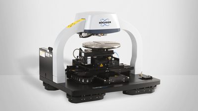
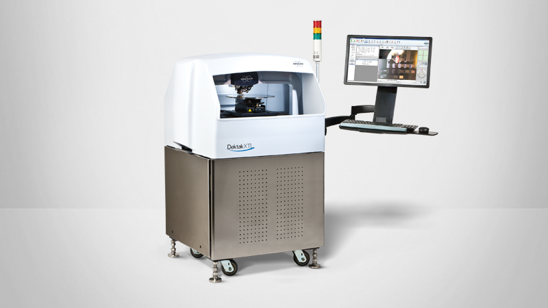
The Dektak brand boasts the first profiler for thin film measurements, the first microprocessor-based profiler, the first profiler with 3D capability, the first PC-based profiler, the first automated 300mm profiler, the first profiler to implement a single-arch design, and the first to harness 64-bit parallel processing architecture. Now, Dektak Pro provides an expanded measurement area up to 200 mm of full-sample access for semiconductor applications, as well as a shortened time to results.
Frequently Asked Questions About Stylus Profilometry Technology
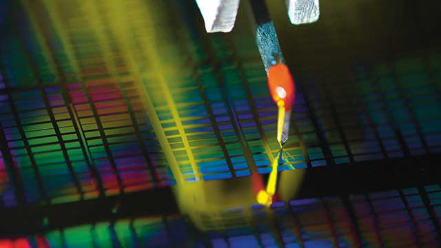
Stylus profilometers trace a low force, sharp tip across the surface to record height as a function of position. From that line trace, surface roughness, step height, waviness, and form can be calculated. Modern systems also support recipe based workflows for these measurements.
LEARN MORE:
Stylus profilers are typically used to measure Ra, Rq, Rz, step height, waviness, and form. Parameters like Ra, Rq, and Rz come from the filtered profile, while step height, waviness, and form are computed from leveled, standardized traces. Proper cutoff selection and leveling are essential so results are comparable across sites and operators.
LEARN MORE:
A stylus force of 1 mg combined with a 2 µm stylus tip will not cause any damage on the majority of surface materials. Sharper styli and very soft materials will require lower stylus forces to avoid scratches. Alternatively a greater stylus radius of up to 25 µm may be used on delicate materials.
Though the native measurement for stylus is a line profile, 3D maps are built by stitching multiple line traces across an area, providing areal visualization and statistics.
Stylus can be a good choice when sample surfaces are transparent or non-reflective surfaces, and when long scan lengths or large vertical ranges are needed. It is also often the most economical path to traceable roughness and step‑height metrology for growing labs. Optical methods often deliver faster 3D areal maps; AFM excels at ultra‑high lateral resolution over small fields of view.
LEARN MORE:
More About Bruker's Dektak Stylus Profiler Systems
The sample is placed on a slider that slides over a highly polished flat glass block. The surface profile is measured by drawing the sample slider at constant speed underneath the stylus tip.
The vertical movement of the stylus tip is measured using LVDT (Linear Variable Differential Transformer) technology, which converts the stylus displacement into a highly precise and linear electrical signal.
Benchtop systems can accommodate small coupons up to full 8” wafers, while production models support large wafers and panels up to 12” size with encoded stages and multi‑site automation. The maximum sample height is 50 mm. Exact limits depend on the model, stage travel, and accessories.
For step height, typical vertical repeatability is on the order of a few angstroms to ~1 nm under controlled conditions, with sub‑nanometer repeatability possible on optimized setups and certified standards. Some key variables affecting accuracy and repeatability are tip condition/geometry, applied force, sample fixturing, vibration/thermal stability, and analysis procedures.
The standard stylus force of a Dektak stylus profiler ranges from 1 to 15 mg. For very delicate materials the force range can be extended downward to 0.03 mg (N-Lite force range).
The Dektak diamond stylus tips have a cono-spherical shape with radii ranging from 25 µm down to very sharp 50 nm. Often, Dektak stylus profilers are equipped with a stylus tip with 2 µm radius which is the recommended stylus radius for roughness measurements.
Sharper styli may be used if higher lateral resolution is required, while styli with greater radii may be useful on very sensitive surfaces.
Dektak styli are easily exchanged within a minute with the included stylus exchange tool. No tiny screwdrivers, Allen wrenches, or tweezers needed. No recalibration needed: Stylus exchange does not affect the calibration of the vertical scale, force scale or optical view.
Every Dektak stylus profiler supports recipe-based workflows for measurement and data analysis. In addition to measurement and automated analysis, Dektak recipes support the acquisition of sample information (e.g., wafer ID and part number), automatic saving of data files using template-generated filenames, and reporting of analysis results (e.g., step heights and roughness) to database tables.
Dektak stylus profilers with motorized XY-stage also allow to generate and run multi-site automation recipes, complete with wafer registration with alignment features (manual or by optical pattern recognition) and automated analysis and database reporting.
Selecting and Upgrading a Dektak Stylus Profiler
- The sub-nm vertical resolution of the LVDT (Linear Variable Differential Transformer) height sensor enables the measurement of heights, depths, and roughness down to single-nanometer levels and below.
- The LVDT sensor technology provides a large vertical range (up to 1 mm) and at the same time very low stylus forces (down to 0.03 mg) with a single sensor head.
- The vertical scale calibration shows excellent long-term stability.
- Moving the sample over a polished flat glass block provides a reference surface that is flat within a few nanometers over the full scan length of 55 mm.
- Dektak styli can be easily exchanged using the included stylus exchange tool without a need for recalibration of vertical range or stylus force.
Lateral resolution is limited by tip radius, so choosing an appropriate tip is important. Steep slopes and narrow features can be misrepresented if the tip cannot access them fully. Very soft or tacky films may require minimal force and specific tips; in some cases, an optical profilometer may bebetter suited.
Bruker provides applications consulting, troubleshooting, and best practice guidance, along with optional service plans for ongoing support, maintenance, and training.
Contact us to arrange a demonstration or submit samples for an evaluation tailored to your test geometry and materials.
Bruker offers upgrade options for users of legacy Dektak systems. Contact us to discuss your current system, measurement requirements, and available options for moving to a current Dektak platform.
Dektak Webinar Series
Our webinars cover best practices, introduce new products, provide quick solutions to tricky questions, and offer ideas for new applications, modes, or techniques.
How Can We Help?

Bruker partners with our customers to solve real-world application issues. We develop next-generation technologies and help customers select the right system and accessories. This partnership continues through training and extended service, long after the tools are sold.
Our highly trained team of support engineers, application scientists and subject-matter experts are wholly dedicated to maximizing your productivity with system service and upgrades, as well as application support and training.