Expansion of 3D Optical Profiler to Wide Field and Rough Samples
Focus Variation extends 3D optical profile measurement capabilities to include rough surfaces and larger fields of view.
This webinar explores how Focus Variation — a non-contact 3D measurement method for fast, accurate areal surface topography measurement — improves operator experience and allows direct, high-quality visualization of wide-field and rough samples.
Webinar Summary
This presentation explores key considerations, necessary capabilities, and technical solutions for navigating the challenges faced by metrology lab managers, quality engineers, and researchers currently using 3D optical profilers in their work. Topics include:
- Principle of focus variation;
- Metrology capabilities & boundaries conditions for best data collection; and
- Using color image information for masking, levelling surface and correlating with topography.
Use case study applications include:
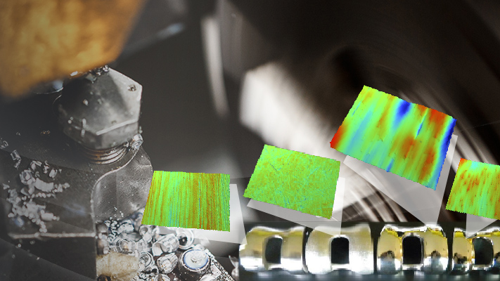
- Tribology (e.g., servicing labs, tribology departments, and failure analysis labs);
- Corrosion testing (e.g., servicing labs, pipe manufacturing R&D, coatings research);
- Aesthetic and Perception Assessment (e.g., automotive interior, fabrics, paper); and
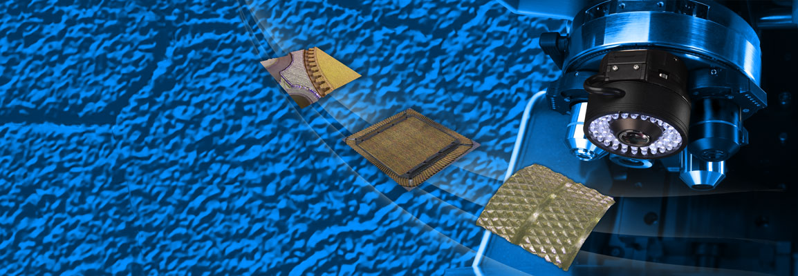
- Additive Manufacturing and 3D Printing (e.g., fine-tuning the manufacturing process, printer and powder/material qualification, quality control).
This webinar was presented on November 11, 2018.
Find out more about the technology featured in this webinar or our other solutions for measuring surface topography at the nano-scale:
Featured Products and Technology

Speaker

Samuel Lesko, Ph.D.
Dir. of Technology and Apps Development for Tribology, Stylus & Optical Profilers, Bruker
Samuel Lesko has over 20 years of optical and stylus profiler applications experience, particularly in using white-light interferometry in a wide variety of fields, from MEMS and semiconductor to automotive and aerospace. He is a member of SME and part of ISO/TC 213/WG committee (areal roughness) and obtained his physics Ph.D. and material science engineering degree at the University of Burgundy in France.