Automated AFM and CIPT Systems
High-Accuracy Probe-Based Metrology Solutions
Bruker's semiconductor metrology portfolio includes automated AFM systems for nanoscale surface characterization and Current In-Plane Tunneling (CIPT) systems for magnetic tunnel junction characterization. Automated AFM systems provide reliable, inline measurement of surface roughness, CMP, and etch-depth features on the most current technology nodes and wafers, with fully automated operation, high repeatability, and low cost per measurement for high-volume production environments. CIPT solutions deliver very fast, cost-effective characterization of magnetic tunnel junctions using non-invasive, microscale probing, enabling accurate resistance measurement, homogeneity control, and rapid device development and testing.
These solutions are used across semiconductor manufacturing and related high-volume production environments where precise nanoscale measurement and inline process control are critical.
Find the Best Probe-Based Metrology Solution for You
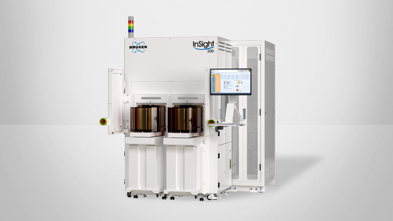
Automated AFM Systems
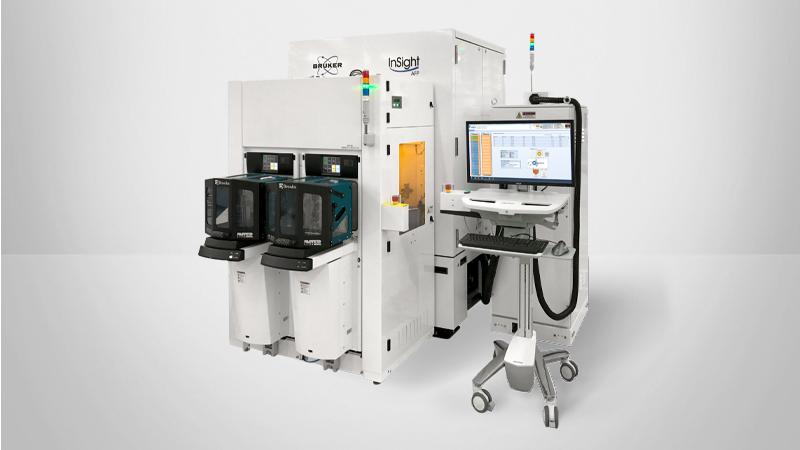
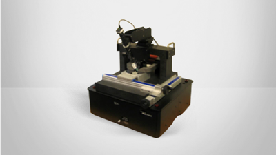
Current In-Plane Tunneling Systems
High-Accuracy Metrology for Semiconductor Production Environments
Bruker’s Automated AFM and CIPT solutions provide high-resolution metrology for semiconductor process development, inline process control, advanced packaging, and large-area surface characterization — from nanoscale roughness, profile, and dimensional measurements to full-die and wafer-scale analysis.
Contact us to discuss your measurement requirements, find out about the systems best-suited for your application, discuss options for system specialization, or request a quote based on your specific needs.

Advanced Process Control & Development
Support development and production optimization of critical front-end and back-end semiconductor processes with high-resolution surface, profile, and dimensional metrology.
- CMP process control and development
- Etch process control and development
- Lithography EUV process control and development
- Sidewall metrology and CD reference
- QA/QC for etch depth

Surface, Defect, & Bonding Characterization
Characterize nanoscale surface properties, defects, and topography that directly impact yield, reliability, and advanced packaging performance.
- Surface roughness metrology for FEOL/BEOL
- CIS and CFA analysis
- Hybrid bonding metrology

Large-Area Topography & Wafer Profile Metrology
Measure topography and profile variations from localized features to full-die and wafer-scale dimensions for process monitoring, bonding readiness, and manufacturing control.
- Bevel edge profiling
- Fast atomic force profiling for large area characterization
Frequently Asked Questions
Frequently Asked Questions About Automated AFMs
Bruker Automated AFM metrology solutions reliably measure surface roughness, chemical mechanical planarization (CMP), and etch-depth features on the most current technology nodes and wafers.
Bruker Automated AFM systems are designed specifically for high-volume production environments, offering the utmost ease of use and the lowest cost per measurement for quality control, quality assurance, and failure analysis.
Bruker's InSight® family of fully automated AFM systems are integrated into production lines, allowing data collection to take place without operator intervention for advanced inline process control.
Automated AFMs provide highly repeatable and accurate roughness, height, and depth measurements ranging from sub-nanometer steps to high aspect ratio trenches, enabling nanoscale defect location and characterization.
Atomic Force Profiling is the most accurate, non-destructive method available for optimizing and monitoring challenging CMP and etch process steps. Direct measurements do not require test structures or models and can be peformed in the active area of the die for the best sensitivity to process variations.

Some common applications are in semiconductor, data storage, polymers and thin films, high-brightness LED and solar materials, and display manufacturing.
Frequently Asked Questions About Current In-Plane Tunneling
Current In-Plane Tunneling is a method used to characterize the properties of magnetic tunnel junctions (MTJs) on thin film stacks on a microscopic scale. These non-invasive measurements greatly speed up development and testing — due to the microsized probe spacings, these measurements can be used for both homogeneity control and parameter characterization.
CIPT uses a four-point probe setup to determine characteristic properties of tunnel junctions by measuring resistance at different probe spacings, placing a set of probes on a full wafer/large sample without conventional techniques for structuring of tunnel junctions.
CIPT measurements can be used for both homogeneity control and parameter characterization.
The Current-In-Plane Tunneling (CIPT) method is a way of measuring the properties of a tunnel junction by placing a set of probes on a full wafer/large sample without conventional techniques for structuring of tunnel junctions. This greatly speeds up development and testing. Also, these non-invasive measurements are local in nature due to the very small (micron sized) probe spacing, which can be used for homogeneity control as well as characterization of a parameter varying over a wafer sized sample.
In CIPT measurements, the (sheet) resistance of a sample is measured using a four-point-probe method. A current is sent through a sample by two probes (I+ and I-), and from the induced voltage drop between two other probes (V+ and V-) the resistance of the sample can be calculated. In the figure below (a) represents the top view of the sample, while (b) represents a cross section of the sample.

If the sample is a tunnel junction, a part of the current will flow through the top electrode, while another part will tunnel through the barrier and flow through the bottom electrode. The amount of current tunneling through the barrier can be changed by changing the distance between the probes, as is shown in the figure below.

When the probes are placed very close together the current will not `have time’ to tunnel down and will mainly flow through the top electrode. When the probes are very widely spaced, the current will divide proportionally between the top and bottom electrode. Therefore, the resistance of the tunnel junction will be higher for smaller probe spacing, and fall off to a lower value at larger spacing as schematically shown in the graph above. By measuring the resistance of the tunnel junction for different probe spacing (by selecting different electrodes on the CIPT probes), a number of data points along such a curve is obtained. Fitting the data yields the characteristic properties of the tunnel junction.
In the figure above, the y-axis represents sheet resistance, while the x-axis represents the distance between probes used for each of the measurements. From this figure the following important parameters can be estimated.
- R(T) = Resistance of the top electrode
- R(B) = Resistance of the bottom electrode
- RA Product = Indication for the resistance of the tunnel barrier
- λ = Characteristic length
- TMR = The relative change in resistance between the top and bottom electrode
CIPT is a very fast and cost-effective method that enables non-invasive measurements, helping to speed up development and testing.
CIPT uses non-invasive measurements and very small-scale probes that allow for very gentle contacts, making them ideal for local (micro scale) electrical measurements.
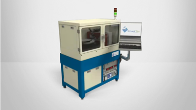
SmartTip CIPT solutions offer several high-field, high-accuracy instruments for both industry and academia to perform CIPT measurements. Both in-plane and perpendicular field options are available.
Bruker's CIPT solutions include low-cost tabletop systems suited for research and development as well as advanced systems for semiconductor R&D and failure analysis, including the ability to map 300 mm wafers with a high perpendicular-to-plane magnetic field.
Frequently Asked Questions About SmartTip Probes
CIPT probes are state-of-art MEMS devices consisting of 12 in-line metal-covered probe fingers (electrodes), each only a few micrometers long and sub-micron width. The very small scale of these probes allows for very gentle contacts, and makes them ideal for local (micro scale) electrical measurements.
CIPT probes are MEMS devices consisting of 12 in-line metal-covered probe fingers, each only a few micrometers long and with sub-micron width, enabling gentle contact and local microscale electrical measurements.
Four different types of probes are available (with mean spacing ranging from 0.75µm to 59 µm). Upon request we can design a probe that meets the requirements for your specific experiment. All CIPT probes are also available on a ceramic carrier which fits into Capres tools.
Users can contact Bruker with their measurement requirements to receive guidance on selecting the appropriate probe for their specific situation.
SmartTip™ CIPT solutions are driven by a mission to develop new frontier MEMS-based nanotechnology microprobes and enable MEMS-based microprobe technologies through collaboration with customers. SmartTip solutions are positioned to advance high-tech nanotechnology-based microprobe applications with a commitment to quality and continuous improvement in development.
Please note that the ability to establish electrical contact with the sample greatly depends on the sample surface. The contact force is generally too small to penetrate an oxide layer, therefore samples should be capped with a non-oxidizing conductor or a metal which forms a conductive oxide (Pt and Ru for example).
Get Expert Answers
Ask us a question, request more information, or get in touch with a Bruker sales representative.