QC-TT
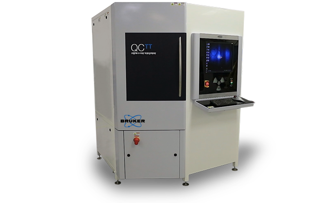

QC-TT Transmission X-ray Diffraction Imaging (XRDI) Inspection System
QC-TT is a comprehensive targeted solution for improving yield and process speed for production wafer monitoring and parameter tuning. Featuring advanced XRDI technology, QC-TT allows detection of non-visual defects (NVD) that cannot be detected by any other production-scale technique. Additionally, with full automation and specialized survey and review modes, this system enables high-throughput detection and depth-located analysis of critical defects on high-value wafers prior to polishing. The result is faster, more reliable feedback earlier in the manufacturing process.
Most Advanced X-ray Diffraction Imaging and Analysis
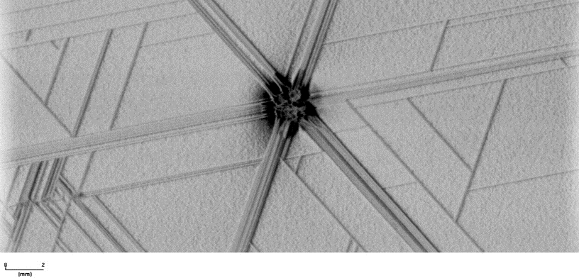
Transmission XRDI enables through-imaging for simultaneous detection of surface and bulk defects with zero edge exclusion. With QC-TT, no killer defects pass undetected in the bulk of the substrate or at non-flat edges.
Detectable defects include:
- Cracks and micro-cracks
- Dislocations
- Inclusions
- Micropipes
- Precipitates
- Slip
- Stacking faults
- Surface scratches
- Sub-grains
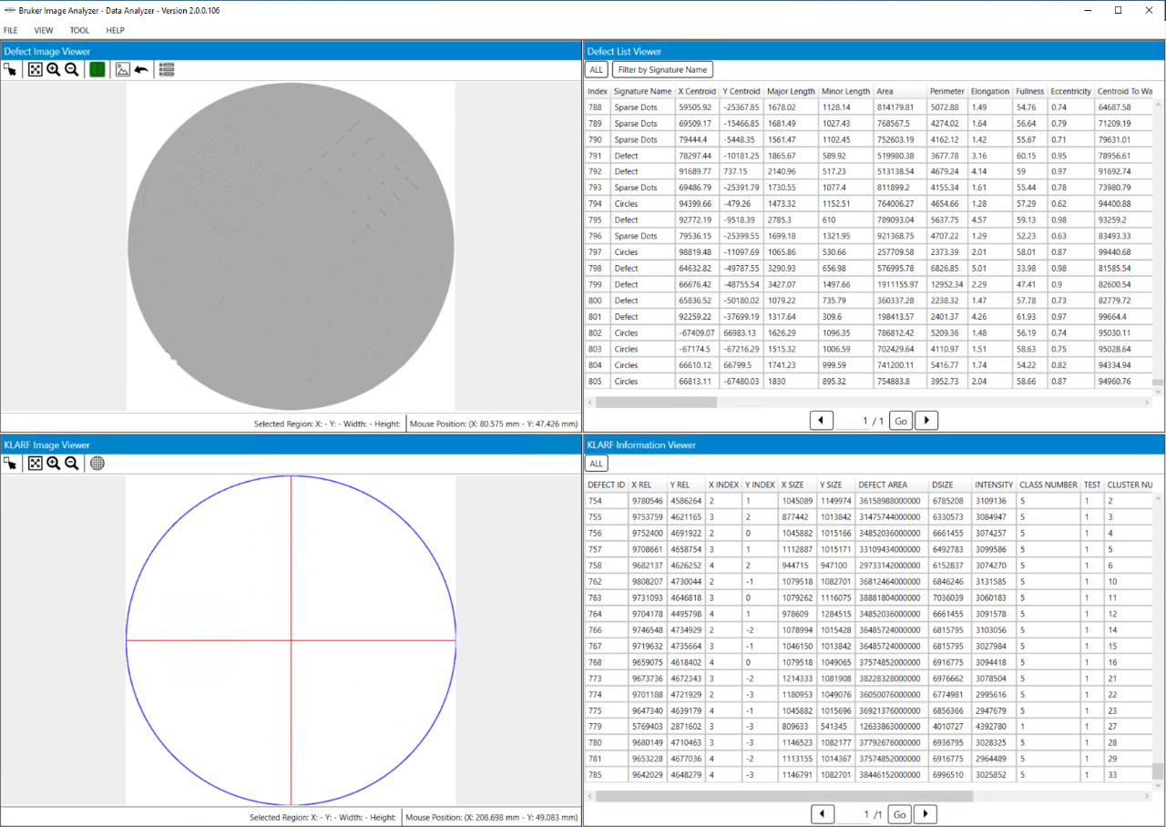
After imaging, the Bruker Image Analyzer (BIA) software enables fully automated data processing and reporting. This defect detection and classification software can classify defects based on one or more of over 30 object parameters, including shape, size, location, intensity, and orientation.
Customizable Automation and Analysis
QC-TT eliminates the need for manual handling and increases productivity through a host of automation capabilities:
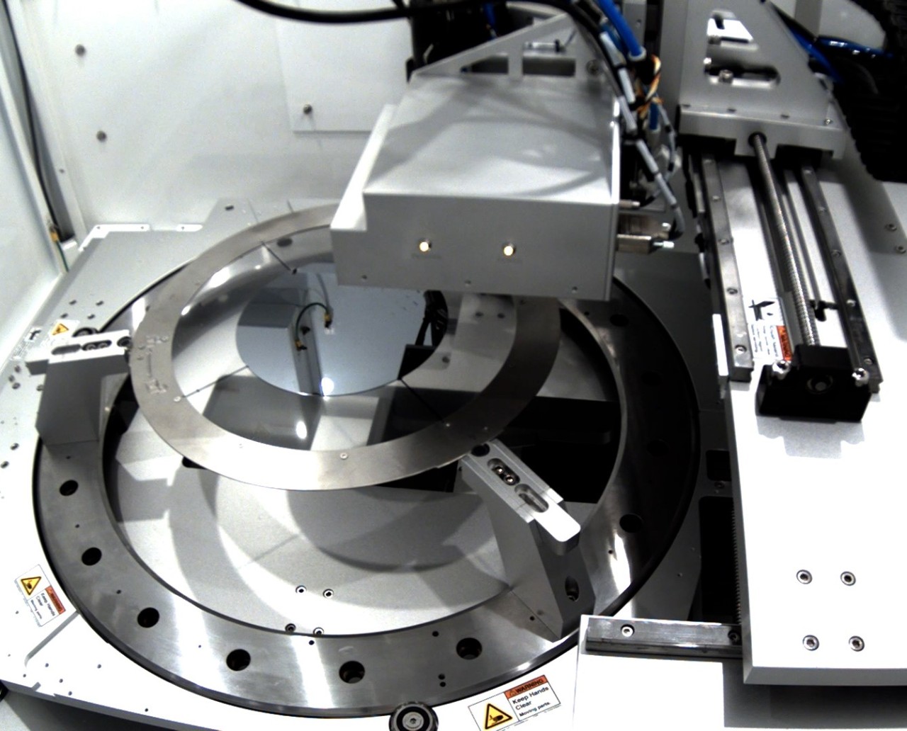
- Wafer loading: Precise, reliable, and repeatable positioning is assured for a range of common wafer sizes, including non-round boule slices.
- Alignment: Specialized algorithms ensure rapid, precise wafer alignment.
- Measurement: Wafers and/or wafer locations are assigned customizable, automated recipes, which can include automated switching between survey, review, and cross-section modes.
- Analysis: In-recipe analysis is customizable to detect the defects that matter to you, with automatic classification and counting.
- Reporting: Reports can be tailored to individual needs, offering a wide range of options, including KLARF reporting, wafer and defect images, detailed defect classification/summary lists, and simple pass/fail reporting.
Specialized Modes for Superior Defect Identification
QC-TT utilizes both high-speed, full-wafer modes and more detailed individual defect review modes to achieve a perfect combination of rapid and accurate failure analyses.
High-Throughput Survey Mode
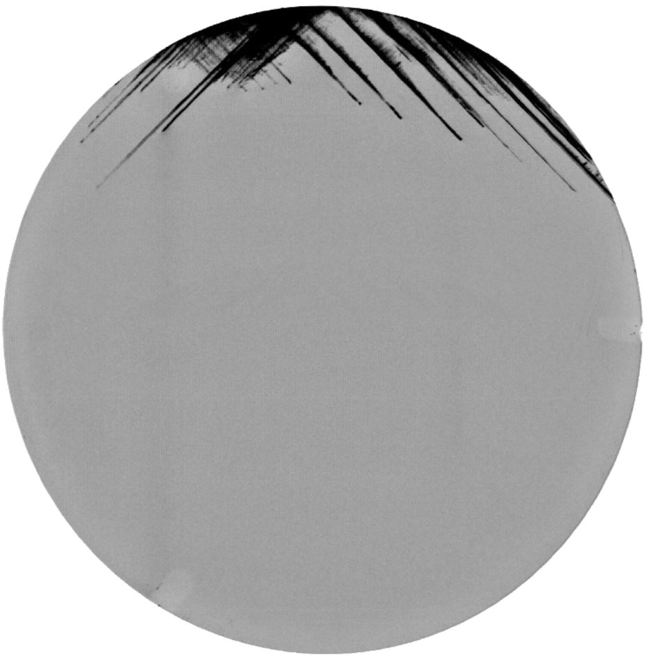
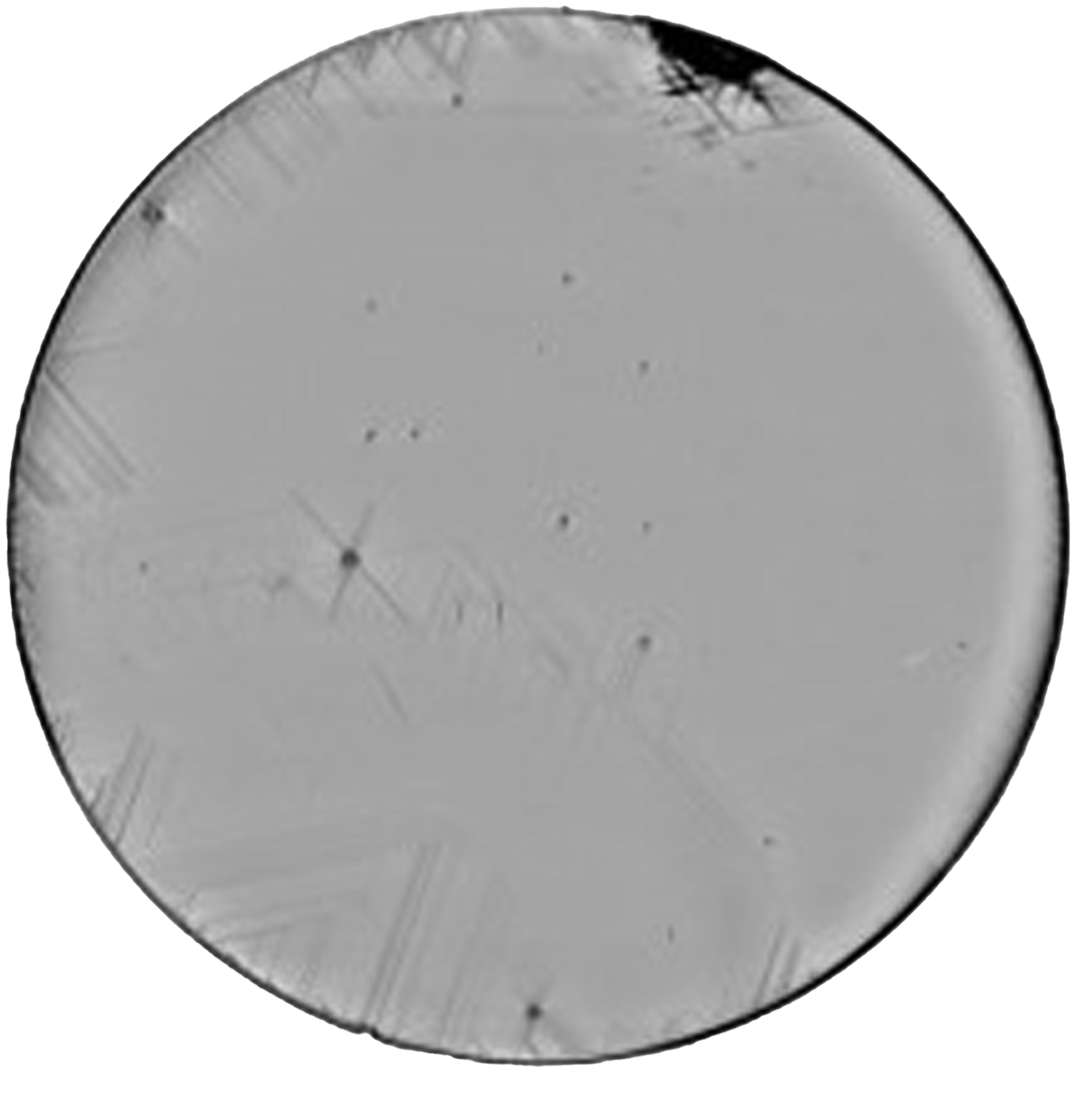
QC-TT can survey up to 15 wafers per hour. These high sampling rates can be invaluable for applications like optimization of ingot slicing for production wafer monitoring and parameter tuning during process ramp.
Combined with fully automated wafer loading, alignment, and measurement, as well as automatic defect detection, defect classification, and KLARF reporting, QC-TT provides the ultimate high-throughput solution for Si production yield improvements.
High-Resolution and Cross-Section Review Modes
QC-TT offers dedicated analysis modes to further investigate the nature and depth-location of individual defects.
- High-resolution review mode uses a high-resolution camera to enable additional detailed examination of individual defects.
- Cross-section review mode creates a virtual wafer cross section to identify approximate depth location of defects.
High-Throughput Production Yield Improvement
Combined with fully automated wafer loading, alignment, and measurement, as well as automatic defect detection, defect classification, and KLARF reporting, QC-TT provides the ultimate high-throughput solution for Si production yield improvements.
Production Wafer Monitoring
Finding the first good wafer from a boule can require multiple rounds of cutting and testing. QC-TT’s high-speed survey can be used to optimize ingot slicing by quickly measuring the length of slip lines, which can be used to predict the location of the next defect-free wafer. This predictive process results in less time and resources being used on cutting and testing of wafers.
Front-End Process Ramp
Parameter tuning can be slow when using low sampling rates or slow characterization techniques. QC-TT offers a high sampling rate with full-wafer survey imaging and is capable of full automation. Using this high-speed imaging with automated defect detection and classification results in a more informed and efficient process ramp.
QC-TT Select Specifications
Each wafer manufacturing facility and semiconductor fab has its own specific requirements and challenges. Our listed product specifications and offerings are always a starting point for a conversation with our experts to determine how our capabilities can meet your needs.
| Survey Mode Throughput (Wafer Dependent) | 300 mm = 7 wph; 200 mm = 10 wph; 150 mm = 13 wph; 4 inch = 14 wph; 3 inch = 15 wph |
| X-ray Tube / Generator | 2.2 kW Mo sealed tube; optional 2.0 kW Ag sealed tube for denser substrates |
| Camera Resolution | 48 µm (survey) and 11 µm (review) pixel size cameras as standard |
| Wafer Size Compatibility | Small coupons and wafers up to 300 mm (manual loading); 2”–200 mm / 200 mm and 300 mm wafers and boule slices (automatic loading) |
Support

How Can We Help?
Bruker partners with our customers to solve real-world application issues. We develop next-generation technologies and help customers select the right system and accessories. This partnership continues through training and extended service, long after the tools are sold.
Our highly trained team of support engineers, application scientists and subject-matter experts are wholly dedicated to maximizing your productivity with system service and upgrades, as well as application support and training.