Application Note: Full-Field Hotspot Detection and High-Resolution Topographic Characterization of Post-CMP Wafers with 3D Optical Profiling
For decades, chemical mechanical polishing (CMP) or planarization has been the predominant technique for smoothing and flattening wafer surfaces during semiconductor integrated chip (IC) fabrication. Post-CMP evaluation is now standard practice for ensuring adequate planarity of the IC layers and confirming compliance with planarity requirements. However, traditional methods of post-CMP process evaluation have analytical limitations that, in light of tightening process control limits, have given rise to a growing need for more accurate wafer surface characterization in semiconductor chip manufacturing. Post-CMP assessment with advanced 3D optical profiler technology presents an optimal alternative, enabling both more accurate and more timely identification of CMP integration issues, thereby reducing the manufacturing costs of meeting the demands of contemporary IC scaling trends.
This application note describes the use of white light interferometry (WLI) for post-CMP wafer characterization, and how advanced packaging manufacturers and CMP specialists can obtain critical data from high-resolution, full-die maps this 3D optical profiling technique makes possible.

Metrology Considerations for CMP
Semiconductor chip manufacturers use CMP both to remove excess dielectrics and metal materials after deposition and between layers to provide adequate surface planarity for the next process step. CMP has become one of the most critical processes involved in chip manufacturing due to the continuous miniaturization of IC transistors. Other recent industry innovations in 3D memory stacking technology (e.g., NAND memory), heterogeneous integration (e.g., CoWos), and advanced packaging have also imposed additional constraints on CMP specifications and increasingly have tightened CMP process requirements.
Manufacturers and CMP professionals often collect localized, small-area surface topography measurements to assess CMP process performance for both QC and reticle inspection. However, because variation in pattern density and size across the die can cause non-uniform planarization, such small-area measurements may not be representative of the full-die CMP topography.1 With high vertical resolution, high throughput, and areal metrology capabilities, Bruker’s WLI-based 3D optical profilers overcome this analytical limitation, easily and quickly collecting large-area surface topography measurements (mm2 to cm2), and delivering full-die maps with angstromlevel vertical resolution and micrometer-level lateral resolution to provide more reliable assessment of wafer surface planarity and CMP process efficacy.2
Full-Die Map via Image Stitching
The core limitations of traditional post-CMP wafer characterization derive from the inability to collect data across the full die, which creates a significant analytical blind spot and unnecessary vulnerability to CMP alignment issues. Today’s most advanced 3D optical profilometers utilize precision stitching algorithms that combine multiple fields of view (FOV) to extend the evaluation length, as well as automatic analyses for rapid, repeatable and artifact-free imaging – even over wide areas.
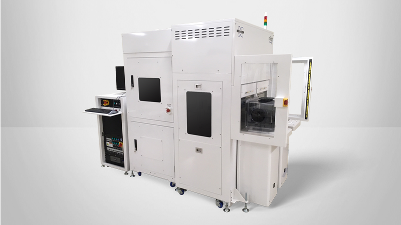
Here, a standard 200m test CMP wafer, which exhibited well-defined structures of varying size, width, and linespacing to simulate a range of topological features, was coated with a 20nm opaque titanium layer to overcome the transparency and dissimilar materials of the wafer surface. This ensured accurate results without compromising surface topography at the die level.3 Measurements were collected with a Bruker InSight WLI optical metrology system equipped with an Equipment Front End Module (EFEM) for automated wafer handling and a Michelson interferometric 5x objective, which provided a large FOV (2.3mm x 1.7mm) combined with 3.6μm effective lateral resolution. Phase shifting interferometry (PSI) mode was selected for data acquisition, as it can achieve angstrom-level vertical resolution at a rapid measurement speed (<3 seconds per measurement cycle).


Note that the automated stitching capability allows extension of the measurement area up to several square centimeters. Additionally, fine camera alignment, together with precise XY motor motion and advanced topography continuity algorithms, ensure height measurement accuracy down to 0.1nm.
Post-CMP Hotspot Detection
Highly efficient CMP processes are optimized for compatibility with the IC design, including in-die pattern density and size variation. This optimization decreases the risk of “hotspot” defects caused by over- or under-polishing at any IC layer, including dishing and erosion, which may degrade lithographic pattern fidelity and cause chip performance variability.4 Consequently, CMP modeling for hotspot detection is an important tool for high-quality and high-efficiency semiconductor chip fabrication.
Under current best-practices for a design for manufacturing (DFM) flow, CMP modeling is widely used for hotspot detection during both front end of line (FEOL) and back end of line (BEOL) processing; to collect pre-CMP and post-CMP profiles from test wafers is central to building suitable models and validating modeling results.5 There are a variety of traditional, commonly-used CMP modeling techniques, including FIB-SEM, TEM, AFM, and stylus profilometry,– however, none of these techniques offer adequate large-area measurement capabilities with both high-resolution imaging and fast throughput.6 WLI bridges the gap between manufacturers’ needs and the capabilities of these other methods, providing access to high-value and previously inaccessible information at full-die level for CMP.
Here, we used WLI for a die-to-die comparison of planarity between test structures located near the edge of the wafer versus the center (see Figure 3, top row). The resulting surface map revealed that edge-located test structures were deeper relative to the surrounding features (indicated by the blue and dark blue tones) than those nearer the center. The surface maps also revealed areas of the substrate with a higher Z-profile (orange in the figure). These results may indicate inconsistency in the CMP process across the wafer and that further CMP process optimization is necessary.
Full die images can also facilitate comparison of the Z-range, or height distribution, of dies; the extremes of such height distributions represent erosion/dishing and protrusion effects. In this case, WLI imaging of the full die revealed disparate height distribution between the edgeand center-located dies, indicating that the CMP process caused hotspots despite performing well at the center die (see Figure 3, bottom row).
Note that this comparison reveals information that other post-CMP evaluation methods relying on small-area “spot” measurements (e.g., T-box) are likely to overlook or be unable to capture, as surface defects can be highly dependent on location, surrounding pattern structure, and pattern density. As a result, traditional in-die spot measurements may reinforce incorrect conclusions about the fidelity of CMP integration and cause manufacturers to miss critical opportunities to correct process parameters. In contrast, WLI mapping provides access to more information on a much larger scale, which better represents the large-area interaction between the polishing pad and the wafer during the CMP process.

Zoom-in View on Full-Die Map
In addition to enabling evaluation of the full die and imaging of the entire wafer, WLI profilers also preserve the lateral resolution of the images while users zoom in on smaller areas of the full-die map. Consequently, users can more closely examine specific areas of interest revealed by full-die mapping, such as CMP hotspots, to better understand the impact of structure density on CMP process efficacy.
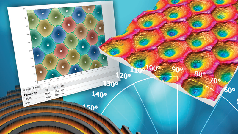
From figure 4, closer examination of test structures revealed that the post-CMP topography varied depending on motif position within the die and structure type (e.g., pad, dense or distant lines, etc.).


Moreover, comparing single-FOV horizontal profiles of the same edge- and center-die locations, measured using a 5x interferometric objective, revealed that the trench depth of the center die reached 48.2nm while the trench depth of the edge die was nearly double that, measuring 94.3nm (see Figure 5).
Quantification of these types of defects yields information suggesting when and where there is a need for improvement in any of a variety of CMP process parameters, such as pressure and speed settings, material selection, wafer internal stress, and more. In this way, high-resolution WLI imaging provides valuable insight into CMP results, which can point to specific, actionable solutions for performance and yield enhancement, and enable easy assessment of experimental plans to optimize the process.
Importance of Specialized Software
The unique imaging capabilities of Bruker’s 3D optical profilometers are augmented by industry-leading Vision64® software integration, which automates WLI imaging and analysis. Using this software, it is possible to simultaneously capture a variety of surface characteristics (e.g., lowest depth, highest peak, area, volume, etc.) for each identified region, and to define measurement thresholds and flag areas of the test structure that do not meet the user-defined tolerance criteria. Moreover, it is also possible to either use the wafer coordinates of an identified region to program a high-resolution single-FOV imaging routine, or to export them into a coordinate map file for defect review by atomic force microscopy.

High-Precision, Full-Die Surface Topography Measurements
Identification and correction of nanometer-level deviation in surface planarity is required for the success of die-todie or die-to-wafer bonding as much as for each IC layer. Consequentially, for full die mapping to be an effective method of post-CMP wafer surface evaluation and a reliable tool for process optimization, it is essential that WLI imaging results consistently achieve 1nm accuracy. A better understanding of the accuracy and repeatability of full-die measurements can be obtained by performing repetitive static post-CMP evaluation experiments in which the resulting data are closely monitored and compared.
Here, 10 static repeats were performed on the center die while monitoring both the Z-height distribution and the mean roughness of the resultant full-die maps (see Figure 7). This short-term repeatability test showed both qualitatively and quantitatively excellent results: Full-die mapping produced the same CMP fingerprint on all test features, and the results exhibited a near-identical height distribution in every instance. Even given the small sample size, the agreement between test runs demonstrated incredible repeatability. Also note that long-term reproducibility on a reference QC wafer has been observed in actual conditions with repeatability of ±1nm over a year.

Conclusion
Bruker’s advanced WLI-based 3D optical profilers demonstrate the capability to measure die-scale (mm2 to cm2 area) nanotopography of semiconductor IC wafers and reticles with high vertical and lateral resolution and short measurement duration (~10 min). Automated measurement and analysis routines provide the high-level throughput, productivity, and consistency required by advanced packaging, imaging, and NAND memory processes. These unique features make Bruker’s WLI technology an ideal solution for validating CMP process design and improving process yield in the research and development phase as well as a strong candidate for process control in production environments.
Authors
- Roger Posusta, Senior Marketing Application Specialist, Bruker Nano Surfaces andMetrology Division (roger.posusta@bruker.com)
- Samuel Lesko, Senior Manager for Optical & Tribology, Bruker Nano Surfaces and Metrology Division (samuel.lesko@bruker.com)
Acknowledgement
Special thanks to SKW Associate, Inc. for providing the CMP test wafer.
References
- F. Dettonia, M.Rivoirea, S.Gaillarda, O.Hinsingera, F. Bertinb, and C.Beitiab,“High resolution nanotopography characterization at die scale of 28 nm FDSOI CMOS front-end CMP processes,” Microelectronic Engineering 113, January 2014, pp 105-108.
- R. Posusta and S. Lesko, “Characterization of CMP Processes with White Light Interferometry,” Bruker application note #564, 2020.
- F. Dettoni et al., "Interferometry: a direct die level characterization technique," ICPT 2012 - International Conference on Planarization/CMP Technology, Grenoble, France, 2012, pp. 1-6.
- D. Woodie, Chemical Mechanical Polishing (CMP), Cornell NanoScale Facility, Cornell University 2007.
- R. Ghulghazaryan, J. Wilson, and A. AbouZeid, “Creating An Accurate FEOL CMP Model,” Manufacturing, Packaging & Materials, Semiconductor Engineering, October 20, 2016.
- C. Beitia, “Challenges in Nanotopagraphy Measurements at Die Level,” FCMN, Monterrey, California, USA, March 21-23, 2017.
©2021 Bruker Corporation. All rights reserved. InSight WLI and Vision64 are trademarks of Bruker Corporation. All other trademarks are the property of their respective companies. AN576, Rev. A0.