High-k Crystallinity
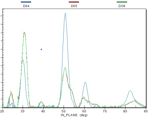
High-K Anneal Skew In-plane XRD
Crystalline properties of the high-k metal gate and other metal / nitride films are critical to the device performance in advanced logic, from finFETs through to nanosheet devices. Using X-ray diffraction it is possible to measure the crystallinity of films. However, high-k films have an additional challenge: typically they are less than 2nm thick.
Bruker Semi have introduced fully automated in-plane diffraction onto their JVX7300LSI system to monitor the grain size and crystallinity of high-k films in a production environment. In the example here, 3 films were grown and annealed at different temperatures. D05 and D06 XRD patterns overlap indicating the same crystalline phase; however sample D04 has a different XRD pattern indicating a phase change in the structure, which can lead to a change in dielectric constant. Additionally, the grain size has increased which will give rise to poorer electrical properties of the high-k layer.
Anisotropic Crystallite Investigation in Ultra-Thin High-K Films
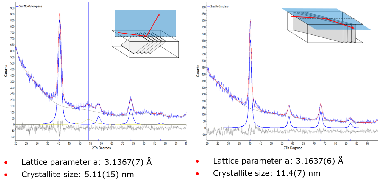
The D8 DISCOVER Plus is Bruker's flagship X-ray Diffraction solution for the analysis of ultra-thin amorphous, polycrystalline and epitaxial films. By applying Coplanar-Diffraction (left) and Non-Coplanar Diffraction (right), the lattice parameters and the crystallite size can be determined with unrivalled accuracy perpendicular as well as parallel to the sample surface. In the presented case of a 5 nm thick Mo film, a high anisotropy in lattice parameter and crystallite size is observed: The vertical crystallite size equals the film thickness, whereas the in-plane crystallite size is more than twice as large (11.4 nm).