Optimizing Semiconductor-based LED Devices Using EDS of Electron Transparent Specimens in STEM and SEM
Nanoanalysis by Energy-Dispersive X-ray Spectroscopy of FIB Lamellae in the Scanning Electron Microscope
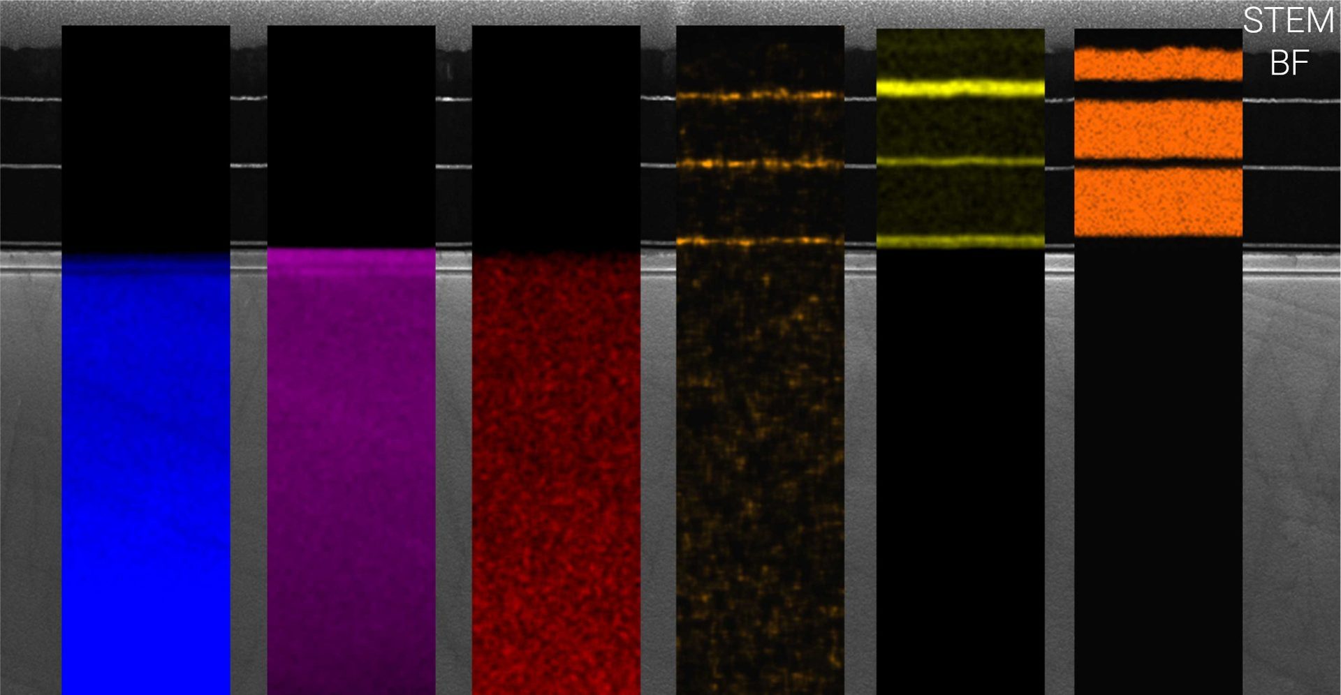
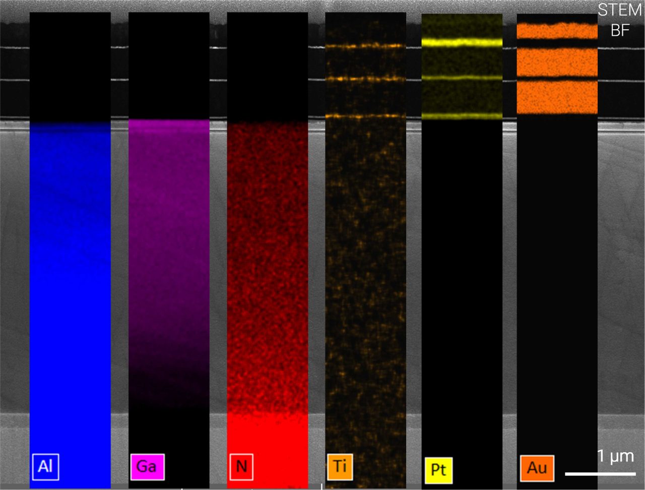
The understanding of semiconductor structures on the nanoscale mostly needs high-end analytical scanning transmission electron microscopy including the respective method combination and complex specimen preparation. As one example for this we present a study of UV-LEDs which have been recently tested for skin-tolerant inactivation of SARS-CoV-2 and multi-resistant bacteria. Optimization of these devices often requires structural and compositional analysis involving STEM-EDXS, EELS and high-resolution imaging. Challenges in quantitative analysis can be introduced by conventional TEM-specimen preparation. Preparation artifacts were identified studying a Si-Ge layer system and minimized by FIB.
And now, what if FIB-prepared specimens could be used for pre-screening and even for some part of the analysis in SEM already?
We explore such alternatives carrying out so-called T-SEM: investigating electron transparent FIB-lamellae in SEM. AlGaN based LEDs were prepared in cross-section by standard lift out technique and investigated by EDS in SEM. Possibilities and limitations for quantifying the composition of semiconductor layer systems in SEM, including element depletion and segregation triggered by morphological substrate defects, will be shown and related to data obtained by STEM.
Who Should Attend?
- Scientists and academics from semiconductor fabrication, including laser and spectroscopy research
- Academic staff and students interested in:
- Semiconducting materials
- FIB
- TEM specimen preparation
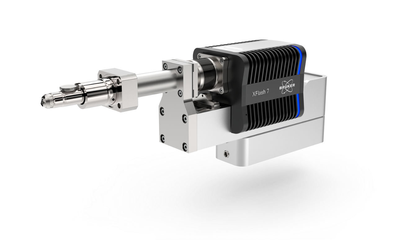
- SEM-, T-SEM and STEM-EDS related analysis techniques
Speakers

Dr. Anna Mogilatenko
Ferdinand-Braun-Institut gGmbH
Leibniz-Institut für Höchstfrequenztechnik and Humboldt University of Berlin

Dr. Purvesh Soni
Sr. Applications Scientist EDS, Bruker Electron Microscope Analyzers
Dr. Igor Németh
Application Scientist EDS, Bruker Nano Analytics
Watch this Webinar On-Demand
Please enter your details below to gain on-demand access to this webinar.