
X-Ray Defect Inspection Systems
Advanced Inline X-Ray Imaging
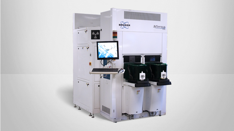
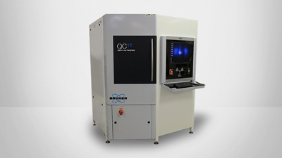
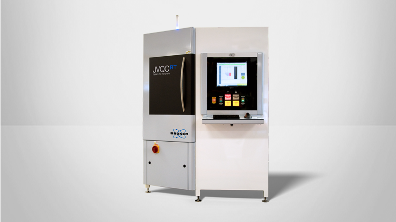
Bruker defect detection systems use X-ray diffraction imaging (XRDI) to detect crystalline defects on single-crystal substrates, such as slip, cracks, dislocations, and micropipes. Operating without the use of etching acids, our non-contact XRDI inspection systems are broadly employed to detect cracks in Si wafers that cause wafer breakage and to improve yield and quality of other high-value substrates such as GaN, CdTe, and SiC.
Find the Best X-Ray Defect Inspection System for You
X-Ray Defect Inspection Solutions for Semiconductor Manufacturing Applications
Bruker's X-ray diffraction imaging (XRDI) solutions support non-contact defect detection and classification for semiconductor substrates, helping manufacturers identify crystalline defects, improve yield, and maintain substrate quality across development and production environments.
Contact us to discuss your measurement requirements, find out about the systems best-suited for your application, discuss options for system specialization, or request a quote based on your specific needs.

Semiconductor & Advanced Packaging Inspection
Support defect inspection and process monitoring in advanced semiconductor manufacturing.
- Advanced packaging defect inspection
- Thin film crystalline defect monitoring
- Warpage and tilt mapping for advanced processors

Crystalline Defect Detection & Monitoring
Help improve yield and quality for high-value semiconductor materials.
- Detect crystalline defects on single-crystal substrates
- Includes: Slip detection, crack detection, dislocation detection, micropipe detection

Electronics Assembly & Quality Control
Support inspection and analysis workflows for electronics assembly applications.
- Wetting behavior analysis for automotive controllers
- Automatic non-wet detection for wireless chips
Get Expert Answers
Ask us a question, request more information, or get in touch with a Bruker sales representative.