Advanced Elemental Analysis of Semiconductors and Microelectronics Using QUANTAX WDS for SEM
Analysis of Semiconductors with Wavelength-dispersive X-ray Spectrometry
Semiconductors are indispensable for many high-tech industrial products including those of our daily life (smart phone, tablet, laptop, car…). Analyses of these materials and products for their elemental composition are often challenging due to particular requirements in resolution, both spatially and spectrally. This webinar will provide information on the advantages of WDS for SEM for the analyses of semiconductor material and related high-tech industrial products, such as microelectronics.
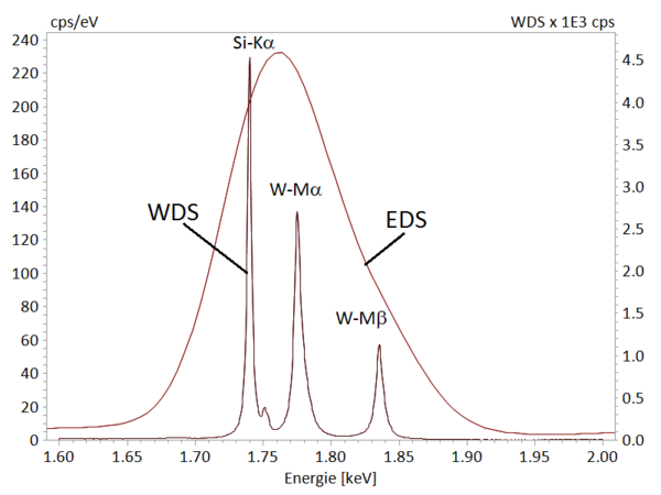
In-situ microanalysis using scanning electron microscopes (SEM) is well established in R&D and QM of semiconductors and microelectronics. Due to its versatility, robustness and speed, energy-dispersive X-ray spectroscopy (EDS) is a suitable analytical technique for many of these applications. However, EDS analysis does have limitations, especially with respect to elemental peak overlaps, which are common in certain semiconductor materials. Accordingly, when higher spectral resolution beyond the limits of EDS is required, wavelength-dispersive X-ray spectrometry (WDS) is the ideal analytical technique for gaining a more detailed insight into the composition of the material.
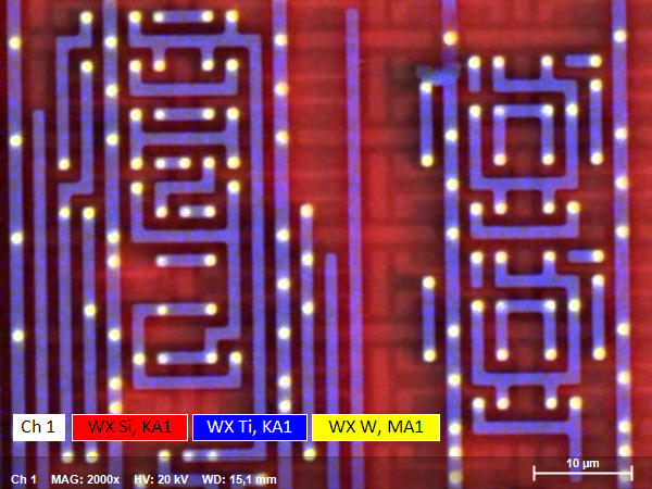
In this webinar, we will present point analyses and element distribution maps of challenging examples. We will focus on some semiconductors with pronounced EDS peak overlaps (e.g. Si-Ta-W, Mo-S and Bi-Pb) where the superior spectral resolution provided by the QUANTAX WDS is striking. Through the mapping inhomogeneities and gradients in the material can be visualized and quantitatively analyzed. It facilitates exact and reproducible determination and quantification of the respective elements in the material systems and related high-tech products.
Who Should Attend
- Material scientists
- Researchers on semiconductors
- Failure analysis experts
- Scientists and lab engineers interested in WDS for SEM
Speakers

Dr. Max Buegler
Application Scientist Micro-XRF, Bruker Nano Analytics
Dr. Michael Abratis
Sr. Application Scientist, Bruker Electron Microscope Analyzers
Watch this Webinar On-Demand
Please enter your details below to gain on-demand access to this webinar.