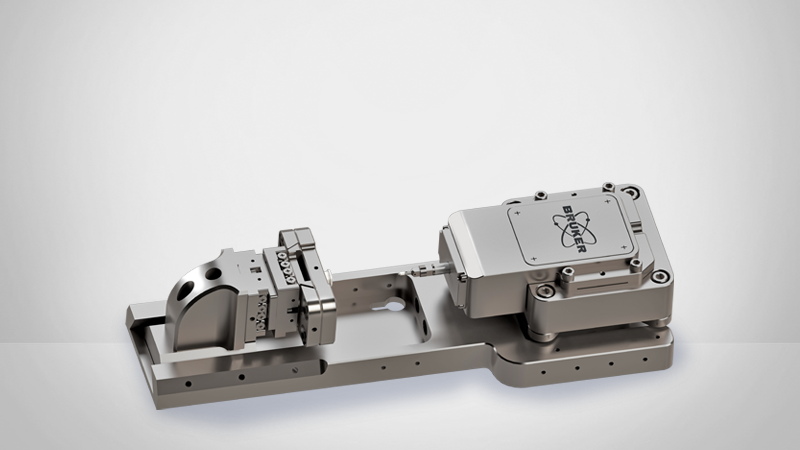
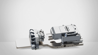
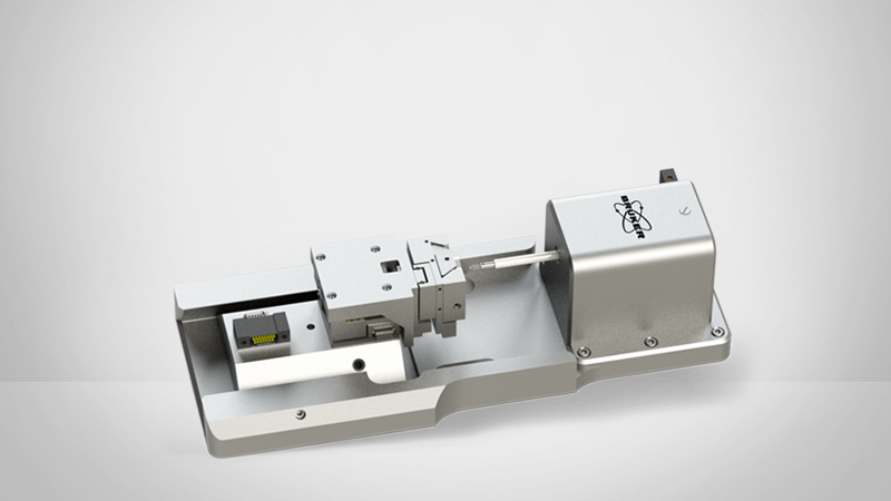
Push-to-Pull Device
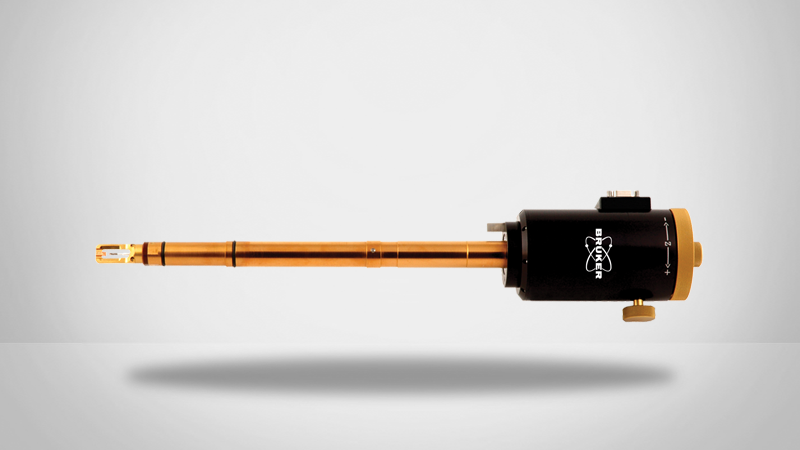
Now that 1D and 2D materials can be rapidly and consistently synthesized, new mechanical characterization techniques are needed to evaluate and optimize their mechanical properties for use in the next generation of products and devices. To address the need to provide a suitable testing platform for these new forms of material, Bruker has developed the Push-to-Pull (PTP) device, which is an in-situ tensile apparatus designed to work in conjunction with the Hysitron PI Series PicoIndenter instruments for SEM and TEM.
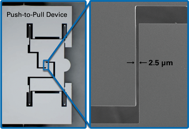
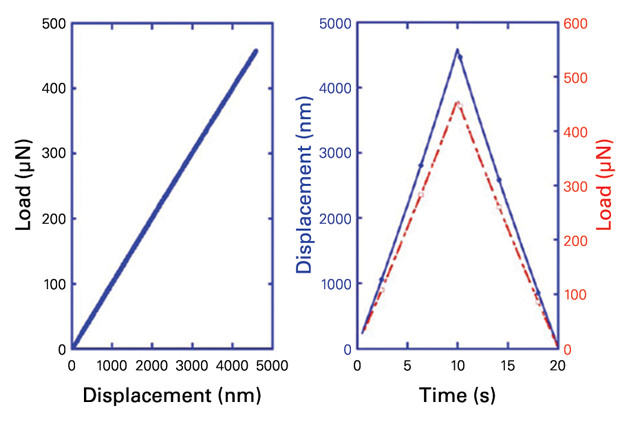
The PTP device is a consumable, MEMS-fabricated flexure device to which a nanotube or thin-film specimen can be mounted. Once prepared, the sample is transferred to the PicoIndenter system and a quantitative tensile load is applied. Mechanical data is used to calculate tensile properties while simultaneous electron microscope imaging provides real time video of the microstructure behavior. An electrical version of the device named the electrical Push-to-Pull (E-PTP) further expands the capabilities and enables four point electrical measurements throughout the tensile experiment.