Application Note: Photothermal AFM‑IR for Semiconductor Materials and Devices
Valuable Nanoscale Insights for the Semiconductor Industry
As device dimensions shrink, the ability to resolve and chemically identify ever‑smaller contaminants becomes increasingly important. Photothermal AFM‑IR, often shortened to just AFM‑IR, is a Bruker‑patented nanoIR technique that allows for chemical identification with spatial resolution below 10 nm and monolayer sensitivity—breaking the diffraction limit by over 100x. This technique is easy to use and straightforward to analyze.
This application note explores how AFM‑IR addresses key challenges in semiconductor development, offering insights into contamination, interfaces, and material performance that are critical for advancing device reliability and fabrication processes.
Readers can expect to find:
- Background information framing the significance of AFM-IR for semiconductor applications
- Working principles description of photothermal AFM-IR
- Six case studies illustrating how AFM-IR answers real research and manufacturing questions
KEYWORDS: Nanoscale Infrared Spectrometers; Nanoscale IR Spectroscopy; nanoIR; AFM-IR; AN209; Bruker; Application Note; Dimension IconIR
Photothermal AFM‑IR is a powerful technique for nanoscale chemical analysis, uniquely suited to the demands of semiconductor research and manufacturing. By combining the spatial resolution of atomic force microscopy with the chemical specificity of infrared (IR) spectroscopy, it enables detailed characterization of materials and structures at the sub‑10 nm scale. This application note highlights how AFM‑IR addresses key challenges in semiconductor development, offering insights into contamination, interfaces, and material performance that are critical for advancing device reliability and fabrication processes.
Photothermal AFM‑IR Technology
As device dimensions shrink, the ability to resolve and chemically identify ever‑smaller contaminants becomes increasingly important. Submicron and nanoscale chemical identification of semiconductor materials is a significant challenge in the research of devices, as well as in process control and failure analysis environments. Semiconductor manufacturers use many techniques to identify chemical components, including scanning electron microscopy coupled with energy dispersive X‑ray spectroscopy (SEM/EDX)1 , confocal Raman spectroscopy2 , and nanoscale IR (nanoIR) spectroscopy3 . Of these techniques, nanoIR stands out with chemical specificity and nanoscale spatial resolution.
NanoIR spectroscopy bridges the gap between conventional IR spectroscopy and atomic force microscopy (AFM). While IR spectroscopy is a powerful tool for chemical characterization, its spatial resolution is typically limited to 3–10 μm due to the Abbe diffraction limit. Conversely, AFM provides high‑resolution topographic and mechanical property maps but lacks intrinsic chemical specificity.
Photothermal AFM‑IR, often shortened to just AFM‑IR, is a Bruker‑patented nanoIR technique that allows for chemical identification with spatial resolution below 10 nm and monolayer sensitivity—breaking the diffraction limit by over 100x. This technique is easy to use and straightforward to analyze. In fact, AFM‑IR spectra can be interpreted just like Fourier‑transform IR spectroscopy (FTIR), using established spectral libraries.
During AFM‑IR operation, an infrared laser first induces localized thermal expansion in the sample. This thermal expansion applies a mechanical force on the AFM probe. The magnitude of this force is directly proportional to the sample’s IR absorption at the illuminated wavelength, enabling the generation of localized IR spectra. AFM‑IR absorption spectra correlate well to conventional bulk IR spectra because they are direct measurements of sample absorption, independent of other complex optical properties of the tip and sample.4
Nanoscale Contaminant Identification
Photothermal AFM‑IR enables high‑resolution chemical analysis of nanocontaminants, a characterization capability that is critical for both wafers and photomasks. Typically, high‑resolution TappingMode AFM is used to locate contaminants, followed by IR absorption mapping at a fixed wavenumber, and point spectroscopy to identify chemical composition.
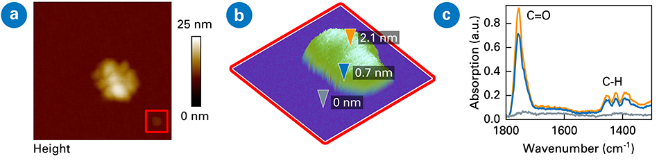
To demonstrate nanoscale chemical characterization capabilities, samples were prepared using known materials typical for semiconductor fabrication environments, which included the polymer nanocontaminant (2 nm height and ~35 nm diameter) shown in the high‑resolution AFM topography review scan of Figure 1a. After the contaminant was located in the review scan, a higher resolution AFM‑IR data scan was collected at 1760 cm‑1 to obtain a chemical map (Figure 1b).
Next, AFM‑IR spectra were collected from three different positions shown in Figure 1c— on the substrate (gray), on top of the contaminant (orange), and towards the edge of the contaminant (blue). IR spectra collected on top of the contaminant and at its edge showed specific functional groups (i.e., C=O and C‑H) that were absent in the substrate spectrum. This data illustrates the capability for photothermal AFM‑IR to be used in chemical identification and mapping of nanocontaminants.
KLARF‑based navigation
KLARF coordinate file–based navigation enables precise targeting of known contamination sites, enhancing both detection and redetection efficiency. By leveraging KLARF navigation, the photothermal AFM‑IR workflow can be streamlined to more rapidly identify and map nanoscale contaminants.
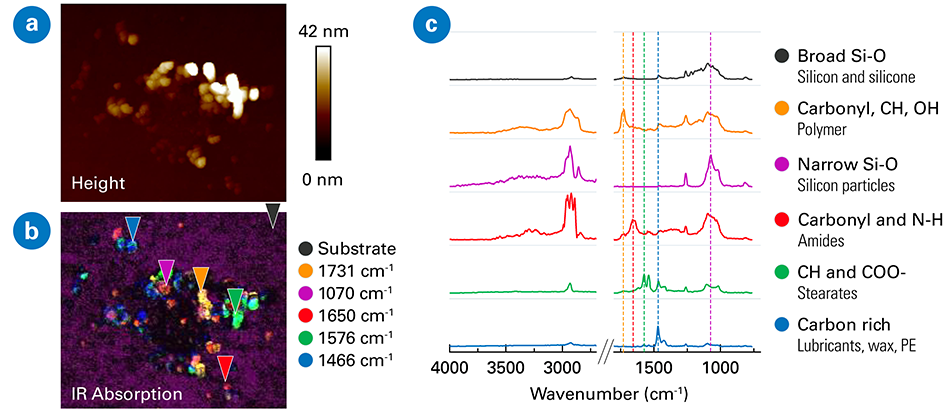
During the example shown in Figure 2, KLARF navigation guided the AFM‑IR system to a cluster of nanocontaminants ranging from 50 to 200 nm in diameter. While topographic AFM imaging alone could not distinguish between different contaminant types, IR maps collected at different wavenumbers revealed five unique chemical functionalities. A composite image of IR absorbtion maps collected at the five distinct wavenumbers shows contaminant distribution (Figure 2b), while spectra collected from each contaminant type enabled clear chemical differentiation (Figure 2c).
Dielectrics
Photothermal AFM‑IR analysis is a complement to other dielectric materials characterization techniques, contributing to a comprehensive understanding of structure‑property relationships. This more complete understanding of dielectric behavior drives improved performance in various applications, including microelectronics, capacitors, and insulators.5
AFM‑IR is used in dielectric materials to identify functional groups, detect impurities, and reveal structural disorder by correlating specific vibrational frequencies to dielectric behavior (e.g., permittivity and loss factor) through spectral analysis. In Figure 3a, an AFM‑IR absorption map collected at 1132 cm-1 on a Si/SiO2 interface reveals high absorption in the SiO2 region, corresponding to the Si‑O‑Si bond
Spectra acquired along a line crossing the interface (Figure 3b) show peak shifts between 1125 and 1134 cm-1, indicating variations in crystallinity or structure near the step edge. These spectral variations can be visualized using color maps that display IR absorption as a function of both position and wavenumber, as in Figure 3c, providing a comprehensive view of chemical and structural changes across the interface.

Thin Films and Coatings
Thin films and coatings are essential to the performance and reliability of modern semiconductor devices, which can require coatings as thin as monolayers. These films serve a variety of roles, from protective barriers and adhesion modifiers to functional layers in lithography, etching, and dielectric patterning
Photothermal AFM‑IR offers a unique capability to chemically characterize these films at the nanoscale, even including monolayer coatings, such as self‑assembled monolayers (SAMs). SAM coatings desensitize surfaces from environmental conditions (e.g., static and adhesion) and serve as a protective layer to prevent device wear and tear.
Figure 4 shows AFM‑IR characterization of a selective SAM coating on top of dense line/space structures. Imaging at 1458 cm-1 (Figure 4b) resulted in high absorption for the C‑H bend in the SAM, and 1068 cm-1(Figure 4c) showed high absorption for the Si‑O dielectric. These IR maps collected at specific wavenumbers therefore easily distinguish between SAM‑coated regions and exposed dielectric surfaces across even this highly complex geometry.

Photoresist Film Analysis
Photoresists are essential materials in semiconductor lithography, where they define patterns on silicon wafers during fabrication. As device geometries shrink and process complexity increases, understanding the chemical and structural behavior of photoresist films becomes critical for enhancing pattern fidelity and minimizing defects.
Photothermal AFM‑IR enables high‑resolution chemical mapping of photoresist films, identifying nanoscale variations in functional groups and molecular structure. This chemical mapping is particularly valuable for evaluating how photoresists respond to exposure and processing, and consequently how they influence pattern formation and resolution. By identifying localized chemical changes, AFM‑IR supports the refinement of lithographic processes and the development of new photoresist formulations, such as metal oxide, chemically amplified, or molecular resists.
Co‑localized chemical and mechanical data can be highly valuable for photoresist films. Resonance Enhanced Force Volume (REFV) AFM‑IR mode offers this multi-channel capability, providing co‑localized, artifact‑free maps of both mechanical properties and IR absorption.6 In Figure 5, REFV AFM‑IR was used to map adhesion, IR absorbance, and height across a 35 nm thick photoresist film that was exposed to a 50 mJ dose. The data, as expected, reveals higher IR absorbance in valleys compared to ridges, and notably illustrates spatial resolution on the 10 nm scale.

Patterned Structures
Patterned semiconductor structures present unique challenges for chemical characterization due to their complex geometries and submicron feature sizes. Photothermal AFM‑IR excels in this context by providing localized chemical information with high spatial resolution. For example, in low‑k α‑SiOC:H/Cu interconnects, AFM‑IR can distinguish between chemically distinct regions within the dielectric layers, even when feature widths fall below the spatial resolution limits of conventional IR spectroscopy.7
Figure 6 shows the interconnect device structure from Reference 7, with alternating copper (Cu) and SiOC:H interlayer dielectric (ILD) layers with a width of the low‑k α‑SiOC:H varying from 1650 nm to 330 nm. IR spectra from targeted locations (marked in Figure 6a), including both Cu and exposed regions of the α‑SiOC:H dielectric, showed clear differences in the C‑H spectral regions of narrow versus wide α‑SiOC:H regions. The decreased intensity of the CH3 mode in the narrow regions of the α‑SiOC:H dielectric is consistent with the loss or modification of terminal CH3 groups during the plasma etch and ashing processes utilized to pattern the dielectric.

AFM-IR Brings Nanoscale Chemical Analysis to Semiconductor Applications
Photothermal AFM-IR offers a transformative approach to nanoscale chemical analysis in semiconductor research and manufacturing. Combining the spatial resolution of atomic force microscopy with the chemical specificity of IR spectroscopy enables direct, localized chemical characterization of nanocontaminants, dielectrics, photoresist, thin films, and coatings. AFMIR provides insights that are inaccessible with conventional techniques, resolving chemical variations at the sub-10 nm scale to support process optimization, materials development, and failure analysis.
Authors
- Cassandra Phillips, Ph.D., Sr Product Manager Nanoscale IR Spectroscopy (cassandra.phillips@bruker.com)
- Chunzeng Li, Ph.D., Sr Engineer Development Application (chunzeng.li@bruker.com)
- Erica Erickson, Ph.D., Materials Science Writer (erica.erickson@bruker.com)
- Jinhee Kim, Ph.D., Applications Scientist (jin_hee.kim@bruker.com)
- Peter De Wolf, Ph.D., Sr Director of Technology and Application Development (peter.dewolf@bruker.com)
- Qichi Hu, Ph.D., Sr Staff Applications Scientist (qichi.hu@bruker.com)
References
- Goldstein, J. I., Newbury, D. E., Michael, J. R., et al. 2018. Scanning Electron Microscopy and X‑Ray Microanalysis. New York, NY: Springer New York. DOI: 10.1007/978‑1‑4939‑6676‑9
- Chen, W.‑L., Lee, Y.‑Y., Chang, C.‑Y., et al. 2013. “Depth‑Resolved Confocal Micro‑Raman Spectroscopy for Characterizing GaN‑Based Light Emitting Diode Structures.” Review of Scientific Instruments 84 (11). DOI: 10.1063/1.4829627
- Mathurin, J., Deniset‑Besseau, A., Bazin, D., et al. 2022. “Photothermal AFM‑IR Spectroscopy and Imaging: Status, Challenges, and Trends.” Journal of Applied Physics 131 (1). DOI: 10.1063/5.0063902
- Dazzi, A., Prazeres, R., Glotin, F., and Ortega, J. M. 2005. “Local Infrared Microspectroscopy with Subwavelength Spatial Resolution with an Atomic Force Microscope Tip Used as a Photothermal Sensor.” Optics Letters 30 (18): 2388. DOI: 10.1364/OL.30.002388
- Sayan, S., Nguyen, N. v., Ehrstein, J., et al. 2005. “Structural, Electronic, and Dielectric Properties of Ultrathin Zirconia Films on Silicon.” Applied Physics Letters 86 (15). DOI: 10.1063/1.1864235
- Resonance Enhanced Force Volume AFM-IR (REFV AFM-IR). Bruker Application Note AN207.
- Lo, M. K. F., Dazzi, A., Marcott, C. A., et al. 2016. “Nanoscale Chemical‑Mechanical Characterization of Nanoelectronic Low‑ k Dielectric/Cu Interconnects.” ECS Journal of Solid State Science and Technology 5 (4): P3018–24. DOI: 10.1149/2.0041604jss
©2025 Bruker Corporation. All rights reserved. Dimension IconIR and PeakForce Tapping are trademarks of Bruker Corporation. All other trademarks are the property of their respective companies. AN209, Rev. A0.