Innovation in AFM: A Timeline of Scientific and Technical Progress
Celebrating 40 Years of AFM
AFM has evolved steadily from its earliest designs to today’s advanced multimodal platforms, as a global community of researchers and engineers continually pushes the limits of AFM applications and technology. They diligently pursue and expand novel uses for the tool, while also developing and integrating innovative hardware. Bruker is immersed in the AFM community, enabling our experts to meaningfully contribute to this expansion of application capabilities and advanced technologies. Along with all who have lent their passion and expertise to advancing this incredibly versatile technique, we celebrate the last forty years of AFM — and look with anticipation toward the next forty.
How AFM has earned its place in modern microscopy
In 1986, a short paper in Physical Review Letters (Binnig, Quate and Gerber) introduced an idea that would reshape microscopy: interatomic forces could be measured with sufficient sensitivity to image the atoms of a surface. Forty years later, atomic force microscopy (AFM) has become one of the most widely used and continuously evolving techniques in nanoscience.
AFM remains a critical technique to modern microscopy — its fundamental working principles (force sensing using a cantilever probe) make it inherently adaptable. It can easily incorporate new detectors, probes, materials, and analysis methods, extending its applicability while retaining the core technique identity of “AFM."
Today, a single AFM can uniquely connect structure, mechanics, electronics, and chemistry at the nanoscale. A fully automated AFM can keep up with high-volume manufacturing needs while providing actionable high-resolution metrology data. A speed-optimized AFM system can capture dynamic biological processes in real time. The last forty years have brought incredible evolution for this platform, and its technological development shows no signs of slowing down.

Extending AFM into New Applications
Researchers across a vast range of applications use AFM to answer cutting-edge research questions. As of early 2026, there are well over half a million publications that mention AFM, and over 147,000 indicate that AFM is a primary component of the research by including it in the title or abstract. A breakdown of average publications per day in each decade shows the rapid growth of AFM over its first 20 years, followed by strong, steady use resulting in ~15 average publications per day.
Below is a curated selection of landmark publications introducing new applications within the early-adoption phase. If these types of novel-application papers are of interest to you, subscribe to our journal club where every month our experts highlight an article that caught their attention.

| Application | Year | Title | Journal | DOI |
|---|---|---|---|---|
| Measurement of magnetic properties | 1987 | Magnetic imaging by ‘‘force microscopy’’ with 1000 Å resolution | Applied Physics Letters | 10.1063/1.97800 |
| Measurement of friction/tribological properties | 1987 | Atomic-scale friction of a tungsten tip on a graphite surface | Physical Review Letters | 10.1103/PhysRevLett.59.1942 |
| Observation of a biological sample in action | 1989 | Imaging crystals, polymers, and processes in water with the atomic force microscope | Science | 10.1126/science.2928794 |
| Manipulation of individual atoms | 1990 | Positioning single atoms with a scanning tunnelling microscope | Nature | 10.1038/344524a0 |
| High resolution imaging of membrane proteins | 1991 | Atomic force microscopy and dissection of gap junctions | Science | 10.1126/science.1910206 |
| Measurement of electrical properties | 1991 | Kelvin probe force microscopy | Applied Physics Letters | 10.1063/1.105227 |
| DNA Imaging | 1993 | Fractured polymer/silica fiber surface studied by tapping mode atomic force microscopy | Surface Science | 10.1016/0039-6028(93)90582-5 |
| High-resolution imaging of protein surfaces in aqueous solution | 1994 | Atomic force microscopy produces faithful high-resolution images of protein surfaces in an aqueous environment | Proceedings of the National Academy of Sciences | 10.1073/pnas.91.3.836 |
| Atomic-resolution imaging of a silicon surface | 1995 | Atomic resolution of the silicon (111)-(7x7) surface by atomic force microscopy | Science | 10.1126/science.267.5194.68 |
| Measurement of chemical properties | 1997 | Chemical force microscopy | Annual Review of Materials Research | 10.1146/annurev.matsci.27.1.381 |
| Single-protein unfolding | 1997 | Reversible unfolding of individual titin immunoglobulin domains by AFM | Science | 10.1126/science.276.5315.1109 |
| Subatomic imaging of a silicon surface | 2000 | Subatomic features on the silicon (111)-(7x7) surface observed by atomic force microscopy | Science | 10.1126/cience.289.5478.422 |
| 10 images/s myosin molecules | 2001 | A high-speed atomic force microscope for studying biological macromolecules | Proceedings of the National Academy of Sciences | 10.1073/pnas.211400898 |
Pioneering AFM Hardware and Modes
Advances in AFM come in many forms, including detection methods and hardware components. A few early milestones introduced via journal articles are listed here:
| Advancement | Year | Title | Journal | DOI |
|---|---|---|---|---|
| Optical lever method | 1988 | Novel optical approach to atomic force microscopy | Applied Physics Letters | 10.1063/1.100061 |
| Fiber optic interferometric detection | 1989 | Improved fiber-optic interferometer for atomic force microscopy | Applied Physics Letters | 10.1063/1.101987 |
| Photothermal excitation to drive cantilevers | 1998 | Photothermal modulation for oscillating mode atomic force microscopy in solution | Applied Physics Letters | 10.1063/1.121224 |
| Small Cantilevers | 1990 | Small cantilevers for force spectroscopy of single molecules | Journal of Applied Physics | 10.1063/1.371039 |
AFM Modes
In many ways, AFM modes dictate what a scanning probe microscope can do. Tens of new modes have been introduced in journal publications, including:
| Mode | Year | Title | Journal | DOI |
|---|---|---|---|---|
| MFM | 1987 | Magnetic imaging by "force microscopy" with 1000 Å resolution | Applied Physics Letters | 10.1063/1.97800 |
| Liquid AFM | 1987 | Atomic force microscopy of liquid-covered surfaces: Atomic resolution images | Applied Physics Letters | 10.1063/1.98374 |
| KPFM | 1991 | Kelvin probe force microscopy | Applied Physics Letters | 10.1063/1.105227 |
| PFM | 1992 | Local poling of ferroelectric polymers by scanning force microscopy | Applied Physics Letters | 10.1063/1.107693 |
| Conductive AFM | 1993 | Spatially resolved electrical measurements of SiO2 gate oxides using atomic force microscopy | Applied Physics Letters | 10.1063/1.108579 |
| Tapping mode | 1993 | Atomic force microscopy of DNA in aqueous solutions | Nucleic Acids Research | 10.1093/nar/21.3.505 |
| Phase imaging with Tapping | 1997 | Phase imaging and stiffness in tapping-mode atomic force microscopy | Surface Science | 10.1016/S0039-6028(96)01591-9 |
| (AFM-based) SThM | 1999 | Scanning thermal microscopy | Annual Review of Materials Science | 10.1146/annurev.matsci.29.1.505 |
| Photothermal AFM-IR | 2005 | Local infrared microspectroscopy with subwavelength spatial resolution with an atomic force microscope tip used as a photothermal sensor | Optics Letters | 10.1364/OL.30.002388 |
| PeakForce Tapping | 2010 | Nanoscale quantitative mechanical property mapping using Peak Force Tapping atomic force microscopy | Microscopy and Microanalysis | 10.1017/S1431927610061829 |
| AFM-nDMA | 2019 | Nanoscale DMA with the atomic force microscope: a new method for measuring viscoelastic properties of nanostructured polymer materials | JOM | 10.1007/s11837-019-03698-z |
| Torsional Resonance Dynamic Friction Microscopy (TR-DFM) | 2024 | Torsional force microscopy of van der Waals moirés and atomic lattices | PNAS | 10.1073/pnas.2314083121 |
Bruker AFM Technology Continues to Shape the Field
Bruker's ever-evolving portfolio of AFMs, modes, and probes has enabled scientists to drive discovery across a nearly countless array of disciplines and applications. Our product offerings include models that are purpose-built to excel in common use cases, plus configuration options to perform specialized experiments. Our catalog of over 50+ materials AFM modes, plus dedicated modes for life science and semiconductor applications, presents a nearly unlimited toolkit for AFM users to fuel their research and innovation. We are also the only major AFM equipment manufacturer that owns and operates a probes nanofabrication facility.
Our dedication to manufacturing quality and cutting-edge probes — coupled with an unsurpassed expertise in AFM — ensures innovative solutions that include instrument, probe, applications assistance, and service support.
SEE OUR INNOVATION MILESTONES:
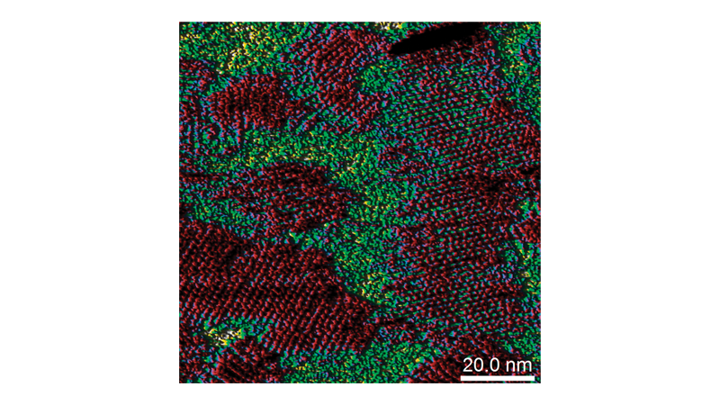
Materials AFMs
Bruker has led the expansion of atomic force microscope capabilities, starting with the introduction of the first commercial system in the 1980s. As the technology has matured, our Materials AFMs have consistently delivered highly reliable high-resolution data and empowered scientists to characterize features on ever more complex samples. Explore some of our milestone innovations, below, download our comprehensive eBook on the use of AFMs for materials research, or see our full catalog of Materials AFMs.
Bruker’s Dimension Icon® brings the highest levels of performance, functionality, and AFM accessibility to nanoscale researchers in science and industry. Building upon the world’s most utilized large-sample AFM platform, it is the culmination of decades of technological innovation, customer feedback, and industry-leading application flexibility.
- Highest-performance tip scanner - Unmatched large-sample resolution with open-loop noise levels, reduced noise floor, and <200 pm drift rates
- Easy productivity - Simple setup, intuitive workflow, and fast time to results for publication-quality data every time
- Versatile open-access platform - Accommodates the widest variety of experiments, modes, techniques, and semi-automated measurements
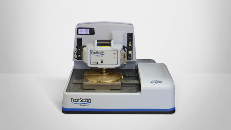
Built on industry-leading Dimension Icon AFM architecture, Dimension FastScan® is the first-and-only high-speed tip-scanning system that achieves frames per second scan rates without compromising resolution or system performance – independent of sample size.
- No-compromise high-speed performance - Highest resolution any time, every time, independent of sample size
- Real-time nanoscale dynamics - Ultimate tip-scanning speed and stability for direct visualization of dynamic behavior
- Automated setup, data acquisition, and analysis - Makes system operation exceedingly simple, while enhancing productivity
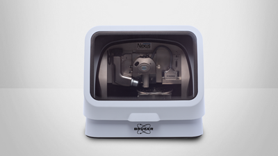
Taking advantage of decades of AFM innovation, Dimension Nexus™ delivers exceptional value, with enhanced upgradability and ease of use. Suitable for both routine and custom experiments and easily upgradable in the field, it is both an excellent starter system and a perfect addition to any AFM lab.
- Best-in-class performance - Powered by the NanoScope 6 controller for lowest noise and highest speeds
- Ultimate versatility and value - Affordable AFM excellence for a wide range of applications and experiments
- Programmable motorized stage - High-throughput, multi-site measurement capability rapidly delivers high-quality data
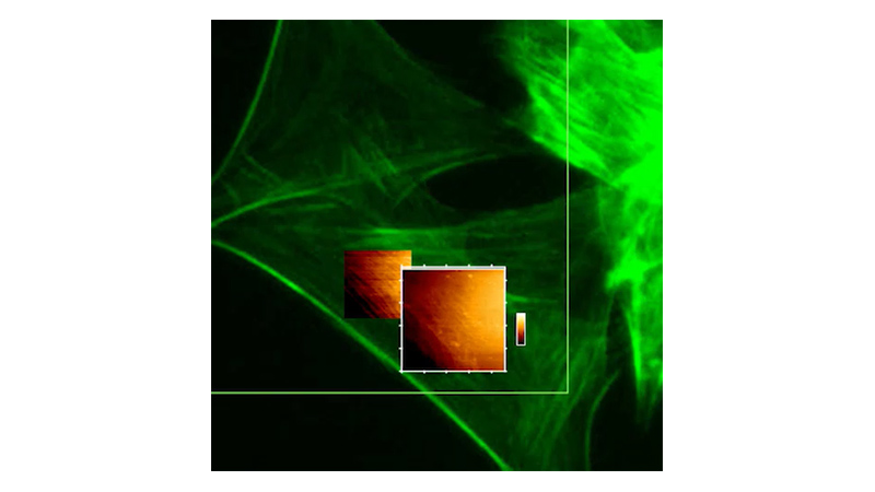
Life Science Research AFMs
Bruker has been helping biologists discover, understand, publish, and advance their knowledge of biological systems ever since our introduction of TappingMode™ expanded AFM use into life sciences research. These instruments deliver the highest quality results for quantitative live-cell mechanical property mapping, highest reoslution molecular and cellular imaging, and fast scanning of dynamic biological processes, as well as seamless integration of AFM with advanced optical microscopy techniques. Explore some of our milestone innovations, below, download the latest edition of our eBook on the use of AFM in life science research, or see our full catalog of Life Science AFMs.
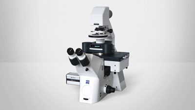
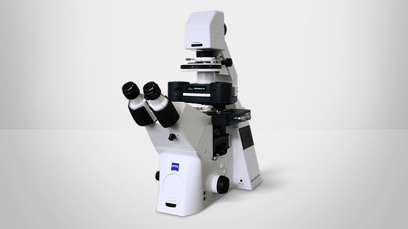
The JPK NanoWizard® V BioAFM combines high spatio-temporal resolution with a large scan area, flexible experiment design, and out-standing integration with advanced optical microscope systems. The automated setup, alignment, and re-adjustment of system parameters opens new possibilities for long-term, self-regulating experiment series.
- Automated setup, workflow, and calibration - New possibilities for long-term, self-regulating experiment series and complex experimental routines
- Advanced force control - Nanomechanical characterization of single molecules, cells, tissues, and highly delicate samples with NanoMechanics quantitative imaging
- 400 lines/sec fast scanning - Real-time dynamic biological process imaging via adaptive, intelligence-based scanning routine, fast force mapping, and molecular recognition
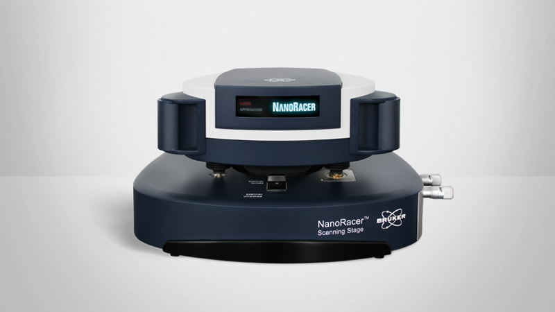
The NanoRacer® High-Speed AFM system delivers an unprecedented imaging speed of 50 frames per second, setting a new milestone in high-speed scanning capabilities to enable true real-time visualization of dynamic biological processes using atomic force microscopy (AFM).
- Ultrahigh 50 fps and 5000 lines/sec scan speeds - Lowest force imaging, minimum sample damage and highest scan speeds for advanced force mapping
- Easy and intuitive use - Cutting-edge engineering, fully automated setup, and state of the art data analysis
- Atomic defect resolution - Real-time visualization of dynamic biological processes with nanometer resolution
Taking advantage of decades of AFM innovation, CellHesion® 300 provides automated, reproducible, quantitative measurements with maximum throughput. It enables correlative and label‑free multiparametric, nanomechanical measurements of living samples in near‑physiological conditions -- creating new possibilities for applications in developmental biology, tissue engineering, nanomedicine, and other areas requiring precise, quantitative characterization of living biological systems
- Improved Productivity - Automated processes and increased sample size deliver the statistical significance necessary in biomedical and pre-clinical research
- SmartMapping Feature - Fast and easy selection of multiple regions of interest over large sample areas with flexible, user-defined 2D shaped force maps
- Label-free Measurements - Multiparametric, nanomechanical characterization of living samples in near-physiological conditions
Photothermal AFM-IR Systems
Utilizing Bruker’s exclusive photothermal AFM-IR technology, our nanoscale infrared (nanoIR) spectrometers offer the world’s easiest to use and most productive nanoscale chemical analysis capabilities. These innovative solutions provide nanoscale chemical identification and material characterization across a diverse range of applications in materials science and life science research. Explore some of our milestone innovations, below, download our comprehensive guide to photothermal AFM-IR, or see the full catalog of Photothermal AFM-IR Systems.
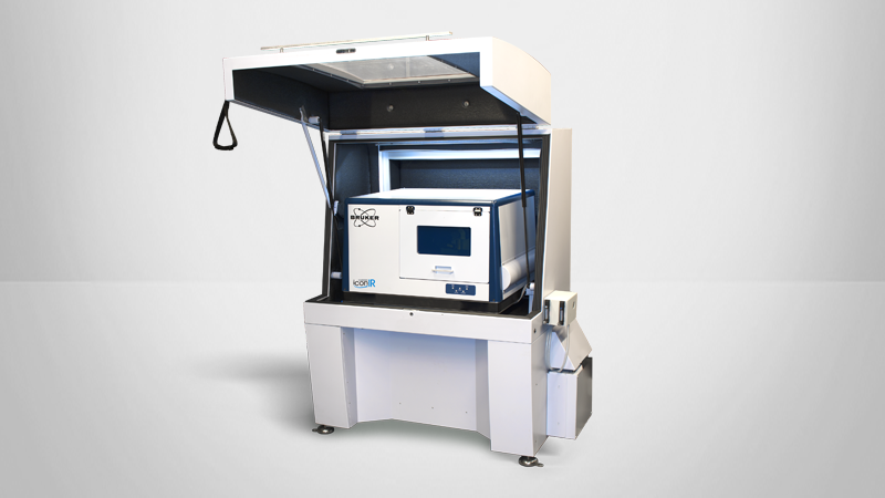
Dimension IconIR™ combines nanoscale infrared (IR) spectroscopy and scanning probe microscopy (SPM) on one platform to deliver the most advanced spectroscopy, imaging, and property mapping capabilities available. This system provides radically more flexibility and applicability to enable groundbreaking research across a broad range of polymer, geoscience, semiconductor, and life science applications.
- Productive guided workflow and programmable stage - Highest measurement throughput with intrinsically easy-to-use AFM-IR
- Multimodal chemical and property mapping - Quantitative nanochemical, nanomechanical, and nanoelectrical data
- Sub-5 nm patented photothermal AFM-IR imaging - Highest resolution, best signal-to-noise characterization with monolayer sensitivity
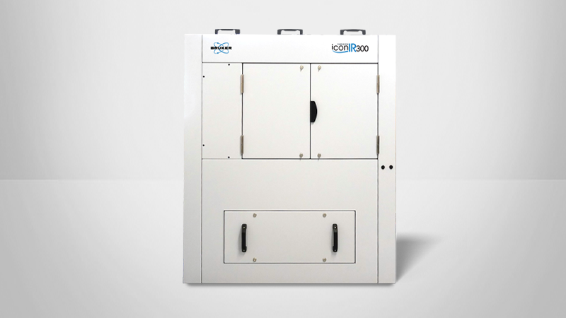
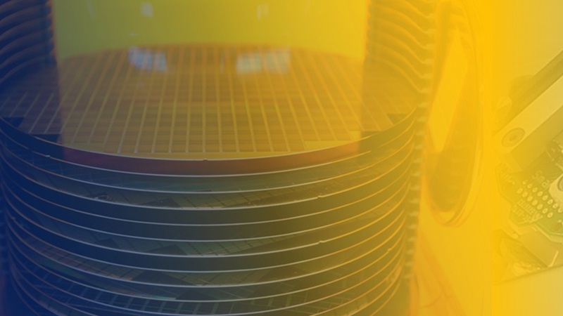
By combining proprietary photothermal IR spectroscopy with advanced AFM property mapping, Dimension IconIR300™ enables automated wafer inspection and defect identification on samples that challenge conventional techniques. The system’s architecture supports rapid chemical imaging and quantitative analysis, extending AFM-IR capabilities to new semiconductor segments and materials.
- Whole-wafer nanoscale chemical and material property characterization -Combined IR spectroscopy and AFM property mapping for highly accurate, non-destructive measurements of 200 mm and 300 mm wafers
- Unambiguous identification of organic/inorganic nanocontaminants - Semiconductor wafer and photomask quality analyzed with photothermal AFM-IR data that directly correlates to FTIR libraries
- Automated recipe-based measurements - User-friendly access to comprehensive data and KLARF file support
Bruker's AFM Modes
Bruker's systems support the world's most complete portfolio of standard, advanced, and proprietary specialized modes. Many of our over 50 modes and variants were either developed or improved by Bruker experts. See some of our unique mode innovations, below, browse our online modes catalog, or download our AFM modes handbook.
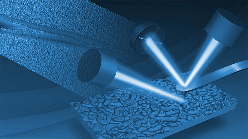
Introduced in December 2009, Bruker’s exclusive PeakForce Tapping® has been the most significant scientific breakthrough in AFM technology since the introduction of TappingMode. It provides unprecedented high-resolution imaging, extends AFM measurements into a range of samples not previously accessed, and uniquely enables simultaneous nanoscale property mapping.
PeakForce Tapping has been widely adopted in materials, data storage, and semiconductor research. PeakForce Tapping and its associated modes ScanAsyst, PeakForce QNM, PeakForce TUNA, PeakForce KPFM, and PeakForce SECM, have been cited in more than 4,000 peer-reviewed publications over the last 10 years, with over 30% of these publications in journals with impact factors in the top 10%.
PeakForce-QI™ mode combines our revolutionary PeakForce Tapping and QI technology to deliver unique quantitative nanomechanical imaging capabilities.
This mode is ideal for investigating the structural and mechanical properties of soft and challenging biological samples under physiological conditions and is only available on our NanoWizard V AFMs.
Though AFM used to be primarily a topographical imaging tool, Bruker has developed modes that measure a host of electromagnetic, thermal, mechanical, chemical, and electrochemical properties. Learn more about AFM-nDMA for viscoelastic measurements, REFV AFM-IR for nanochemical analysis of challenging samples TR-DFM for increased sensitivity to lateral forces, DataCube for hyperspectral measurements, and many more modes.
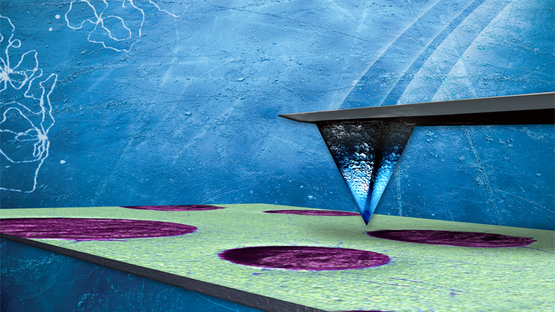
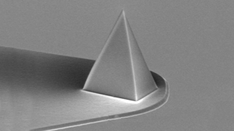
Bruker AFM Probes
As the only major AFM equipment manufacturer that also owns and operates a probes nanofabrication facility, Bruker is uniquely positioned to address your evolving research needs. Our silicon and silicon nitride probes are ideal for general-purpose imaging in air and fluid, while our specialty probes are ideal for more complex experiments, such as measuring electrical or mechanical properties of materials. See some of our most significant probe innovations, below, or browse our online store.

Bruker’s pre-calibrated probes enable intrinsically accurate nanomechanical measurements with no reference samples. Simply read the QR code, confirm the probe number, and measure.

We have developed probes that optimize AFM system performance and data quality; probes that extend AFM capabilities; and probes that have enabled first‑and‑only applications.
For example, our FASTSCAN probes are designed specifically to take full advantage of the Dimension FastScan's extreme imaging speed without loss of resolution or force control. The PR-UM-TnIR probes feature front and back-side gold coating for nanoscale infrared spectroscopy.
Automated AFMs
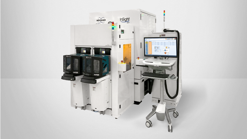
Bruker automated atomic force microscopes (AAFMs) have a long-standing reputation as a reliable solution for semiconductor fabrication facilities globally. From the initial fully automated 200 mm fab AFM to the current InSight 300, Bruker has pioneered patented AAFM innovations that have facilitated the ongoing advancement of next-generation semiconductor devices. Explore some of our milestone innovations, below, or see our catalog of automated AFMs.
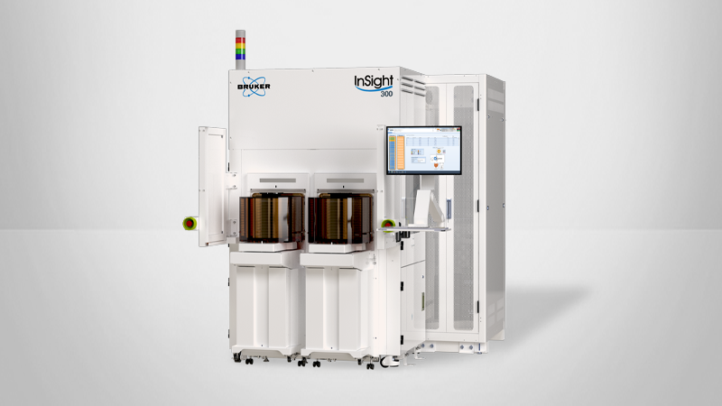
InSight® 300 leverages Bruker’s two and a half decades of experience developing AFM innovations that improve resolution, stability, versatility, and ease of use. This fab-ready automated atomic force microscope (AAFM) is designed for reliable, cost-effective inline metrology in high-volume semiconductor manufacturing environments.
Its exceptionally high throughput, accuracy, and reliability ensure trustworthy results at a low total cost of ownership.
- Best-in-class accuracy and stability - High-performance tip scanner combined with Bruker's ultra flat profilometer stage for nanometer-level precision
- Trusted reliability - 25 years of Bruker's dedicated fab technology guarantees the best solution for HVM environments
- <5 minute recipe creation - Ease of use through dedicated application modes ensures accurate metrology data by any user any time
InSight® AFP is the world’s highest performance and industry preferred CMP profiling and etch depth metrology system for advanced technology nodes. The combination of its modern tip scanner with inherently stable capacitive gauges and an accurate air-bearing positioning system enables non-destructive, direct measurements in the active area of dies.
- NIST-traceable reference metrology - Long-term stability of 0.3 nm over one year
- Highest productivity for inline applicaitons - Reduced MAM times and optimized wafer handling maintain up to 50 wafers/hour throughput
- Up to 36,000 µm/sec profiling speed - Rapid high-resolution 3D characterization with hot-spot identification
There's Always More To Explore
Bruker has deep experience and expertise in all things related to atomic force microscopy, and we are eager to share this knowledge with the larger research community. Browse our atomic force microscopy resource library, below, to learn from our experts.


Contact A Bruker Atomic Force Microscopy Expert
Ask us a question, request more information, or get in touch with a Bruker sales representative.