ZH
My Bruker
联系我们
产品与解决方案
应用
服务与支持
新闻和活动
关于我们
职业
请至少输入2个字符 (您当前输入的是1个字符) 。
Languages
Deutsch
English
Español
Français
Italiano
Polski
Português
Русский
中文
日本語
한국어
▶ Watch On-Demand | 53 Minutes
Using Nanoelectrical Solutions to Expand the Capability of AFM
Innovative nanoelectrical AFM modes provide a significant new capability for materials characterisation
您需要接受 cookie 才能播放该视频。
Cookie 设置
Presented by Peter De Wolf, Ph.D., Worldwide Application Director, Bruker Nano Surfaces & Metrology (March 29, 2018)
Featured Products and Technology
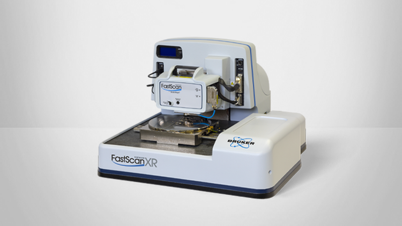
Dimension Icon
Proven highest performance and versatility in an easily tunable AFM platform — now available as IconIR-ready
阅读更多
Dimension XR
Turnkey AFM systems that deliver unique, first-and-only modes and capabilities for advanced materials research
阅读更多
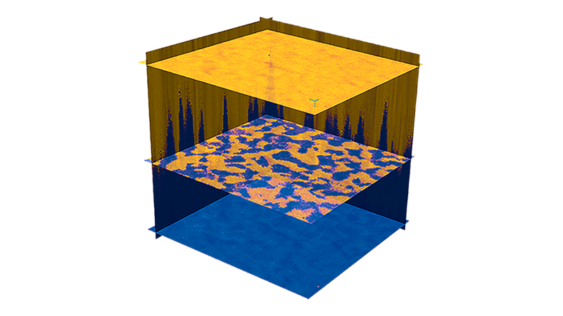
DataCube Modes
Most complete array of electrical AFM techniques
阅读更多
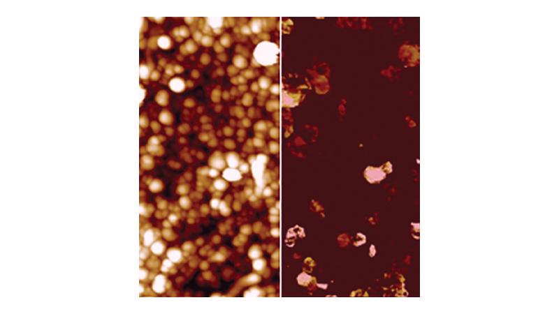
Electromagnetic Modes
Electromagnetic modes are used to characterize the nanoscale electrical and magnetic properties or responses of a surface.
阅读更多
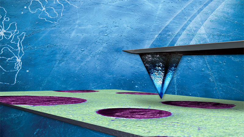
AFM Modes
AFM modes and the broad capabilities from AFM beyond imaging
阅读更多
AFMs for Materials
Bruker's materials research atomic force microscopes, powered exclusively by PeakForce Tapping® technology, are helping researchers advance new nanomechanical, nanoelectrical, and nanoelectrochemical research, on the order of three peer-reviewed published articles per day.
阅读更多
E-Book: The Definitive AFM Modes Handbook
Everything you need to understand, select, and apply AFM techniques in materials research.
下载 PDF
RETURN TO SESSION OVERVIEW