EN
My Bruker
Contact Expert
Products & Solutions
Applications
Services & Support
News & Events
About
Careers
Please use at least 2 characters (you are currently using 1 character)
Languages
Deutsch
English
Español
Français
Italiano
Polski
Português
Русский
中文
日本語
한국어
▶ Watch On-Demand | 53 Minutes
Using Nanoelectrical Solutions to Expand the Capability of AFM
Innovative nanoelectrical AFM modes provide a significant new capability for materials characterisation
You need to accept cookies to play this video.
Cookies Settings
Presented by Peter De Wolf, Ph.D., Worldwide Application Director, Bruker Nano Surfaces & Metrology (March 29, 2018)
Featured Products and Technology
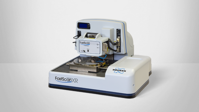
Dimension Icon
Proven highest performance and versatility in an easily tunable AFM platform — now available as IconIR-ready
Read More
Dimension XR
Turnkey AFM systems that deliver unique, first-and-only modes and capabilities for advanced materials research
Read More
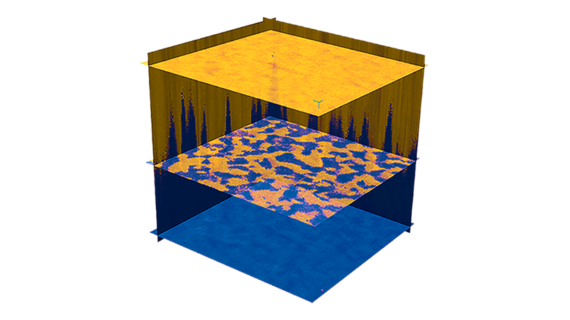
DataCube Modes
Most complete array of electrical AFM techniques
Read More
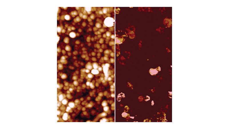
Electromagnetic Modes
Electromagnetic modes are used to characterize the nanoscale electrical and magnetic properties or responses of a surface.
Read More
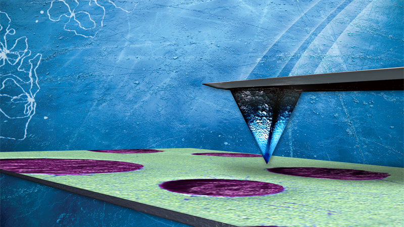
AFM Modes
AFM modes and the broad capabilities from AFM beyond imaging
Read More
AFMs for Materials
Bruker's materials research atomic force microscopes, powered exclusively by PeakForce Tapping® technology, are helping researchers advance new nanomechanical, nanoelectrical, and nanoelectrochemical research, on the order of three peer-reviewed published articles per day.
Read More
E-Book: The Definitive AFM Modes Handbook
Everything you need to understand, select, and apply AFM techniques in materials research.
Download PDF
RETURN TO SESSION OVERVIEW