Dimension IconIR300 纳米红外光谱仪

Dimension IconIR300
Dimension IconIR300™大样品纳米红外系统为半导体应用提供高速、高精度的纳米级表征,具有优秀的测量能力、样品尺寸和材料类型灵活性。通过其专利的光热红外光谱技术和纳米级原子力显微镜(AFM)性质成像能力的结合,IconIR300 能够实现自动化晶圆检测和缺陷识别,适用于最广泛的晶圆和光掩模样品测量。该系统显著扩展了AFM-IR技术在半导体行业的应用范围,超越了传统技术所能达到的领域。
IconIR300建立在Dimension IconIR系统开创性大样品架构之上,提供相关显微镜和化学成像,与传统技术相比增强了空间分辨率和灵敏度。可与自动化晶圆处理和先进的数据收集/分析软件集成,该系统可节省时间和成本,提高生产效率。
To learn more, continue reading, contact us, or see FAQs about this product.
半导体行业的超凡纳米红外光谱和化学成像
On仅Dimension IconIR300系统提供:
- Whole-wafer, non-destructive measurement of 200 mm and 300 mm wafers;
200mm和300 mm晶圆进行全面、无损测量
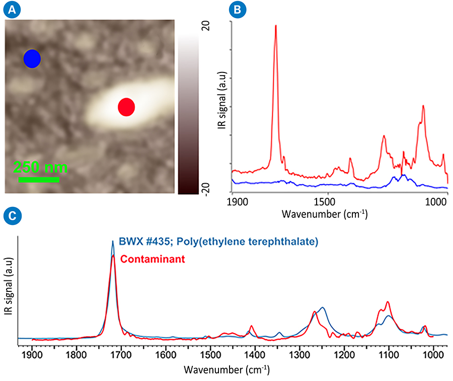
- Unambiguous identification of organic and inorganic nano-contaminants on semiconductor wafers and photomasks with data directly correlating to FTIR libraries;
识别半导体晶圆和光掩模上的有机和无机纳米污染物,数据直接与FTIR库相关联分析
- Non-destructive step-height measurement and nanoscale material property mapping; and
无损台阶高度测量和纳米级材料性质成像;以及
- Automated, recipe-based measurements and KLARF file support for user-friendly access to comprehensive data.
自动化、程式化测量和KLARF文件支持,方便用户访问全部数据。
200mm和300 mm晶圆的全面测量
配置布鲁克专利、独特的AFM-IR模式和专有的PeakForce Tapping®性质成像模式,结合IconIR300的大样品架构,为最广泛的半导体应用提供大的样品灵活性。IconIR300提供直径高达300 mm样品的全面测量,包括各种厚度和材料类型的样品,例如:
- 有机和无机样品
- 图案化的晶圆
- 裸晶圆
- 光掩模
- 数据存储介质晶圆
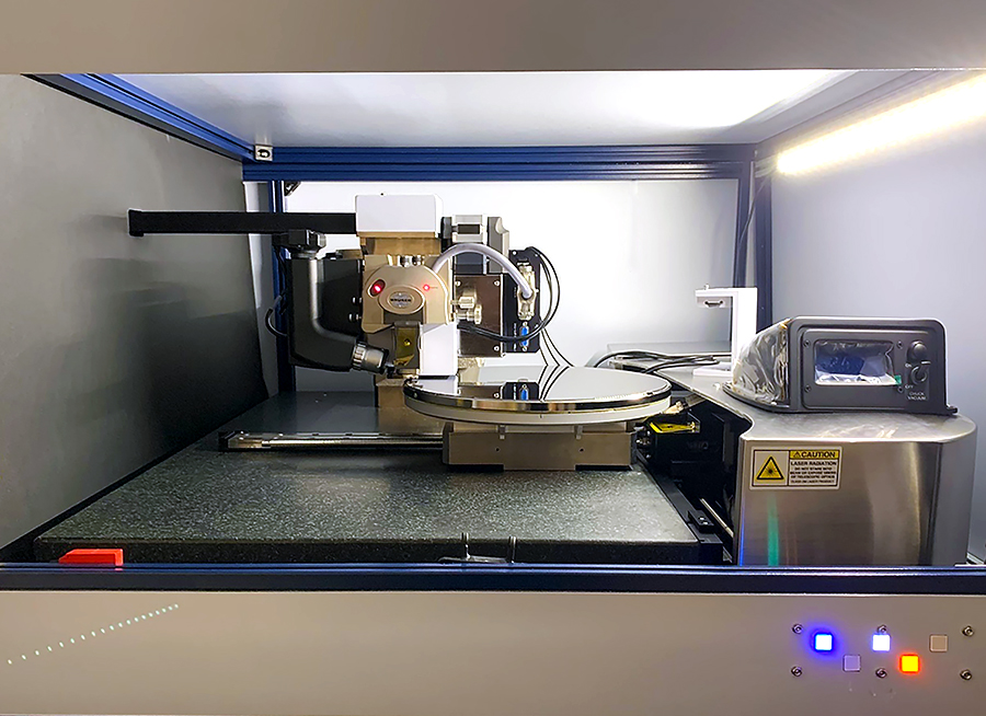
Push-Button AFM and AFM-IR Imaging Automation

Bruker’s AutoMET software on Dimension IconIR systems provides the only AFM-IR measurement automation capability on the market. It supports recipe-driven, push-button nanoscale chemical imaging, AFM imaging, and KLARF-based navigation. IR spectroscopy steps can also be inserted into automated imaging recipes.
AutoMET recipes allow the user to:
- Choose sites of interest
- Define measurements per site
- Set analyses per measurement
This level of automation is essential for routine industrial applications, from semiconductors to pharmaceuticals and polymers. Key benefits include:
- Increased throughput without repetitive manual imaging setup
- Consistent data acquisition from operators of any experience level
- Customizability for a large breadth of materials and analysis needs
半导体应用的高性能纳米级红外光谱

AFM-IR是纳米红外领域的首选技术,Bruker是光热AFM-IR纳米红外光谱技术的创新者。
Dimension IconIR300提供:
- 高精度、丰富、详细的纳米光谱,与FT-IR光谱一致,实现纳米级薄污染物测量;
- 支持各种样品的多种高级测量和操作模式,适用于工业和学术用户;
- 半导体应用中领先的高性能AFM-IR光谱技术;以及
- 用于聚合物薄膜的可靠表面灵敏化学测量
晶圆和光掩模上的高分辨率化学成像
Dimension IconIR300基于行业领先的AFM性能和Bruker专利的Tapping AFM-IR成像技术,提高了纳米红外技术的空间分辨率和样品尺寸的适用范围。
Dimension IconIR300提供:
- 优于10 nm空间分辨率的化学成像,用于各种样品类型的化学成像,包括有机和无机污染物;
- 提供一致、可靠、高质量的数据;以及
- 独特的AFM-IR技术,用于消除全部机械伪影,确保只收集真正的化学成分信息。

高度自动化的纳米污染物识别
关键自动化能力包括:
· 台阶高度测量以及纳米级材料性质成像
· 光学和AFM图像的图案化识别
· 探针位置校正
· 支持全晶圆或网格成像
· 图像定位精度在几十纳米以内
· 复杂、简单的程式化编写;以及
· KLARF文件导入能力,支持纳米红外自动化测量
这些能力,结合具有高分辨率红外光谱的纳米级化学表征,使学术和工业用户能够克服传统半导体材料缺陷识别的限制。
Dimension IconIR300 for Nanoscale Chemical and Surface Analysis
The Dimension IconIR300 is designed for nanoscale chemical identification and property mapping on full semiconductor wafers. By combining photothermal AFM‑IR spectroscopy with the industry‑leading Dimension Icon AFM platform, the system enables non‑destructive, whole‑wafer analysis with direct correlation to FTIR spectra. It is optimized for applications that require precise localization, high chemical sensitivity, and correlative nanoscale measurements across large samples.
Representative use cases include:
- Automated identification of organic and inorganic nano‑contaminants on 200 mm and 300 mm semiconductor wafers and photomasks
- Nanoscale defect characterization, linking composition with topography and material properties
- Chemical imaging of polymer residues, thin films, and patterned materials, including block copolymers and surface contaminants
- Surface‑sensitive nanoscale IR spectroscopy for polymeric and thin‑film materials
- Correlative chemical and material property mapping, combining nanoIR spectroscopy with PeakForce Tapping–based nanomechanical measurements
- Recipe‑based, high‑throughput wafer analysis, including defect navigation via KLARF file import and automated measurement workflows
LEARN MORE:
Chemical ID of Polystyrene Contaminants
In this real‑time demonstration, a Bruker nanoIR applications expert highlights the semiconductor‑focused capabilities of the Dimension IconIR300 through nanoscale defect identification on a full 300 mm wafer.
- Walks through IconIR300 hardware, including 300 mm wafer loading, alignment, navigation to defect sites, and tip engagement.
- Analyzes sample with 150 nm pitch structures and ~50 nm polystyrene particles, including particles on ridges and inside trenches.
- Shows strong agreement between IR images and topography, with zoom‑in views of nanoscale contaminants.
- Confirms that all particles share the same chemical identity, with intensity differences driven by particle size.
- Correlates nanoscale spectra with known FTIR signatures for material identification.


Frequently Asked Questions
Yes, this system is purpose-built for photothermal AFM-IR and property mapping on 200 mm and 300 mm wafers. It supports recipe automation and defect mapping for semiconductor workflows.
IconIR300 can detect and chemically identify both organic and inorganic nano-contaminants on wafers and photomasks. Its AFM-IR spectra can be directly correlated with FTIR reference libraries.
Yes. Dimension IconIR300 supports Bruker’s AutoMET® software and KLARF-based navigation. This enables user-defined automated nanoscale measurements at user-defined locations on wafers, grids, or arrays of multiple samples. IR spectroscopy steps can also be inserted into automated imaging recipes.
AutoMET® recipes allow the user to choose sites, then define measurements per site and analyses per measurement. This capability is essential for routine industrial applications, from semiconductors to pharmaceuticals and polymers.