Dimension IconIR300

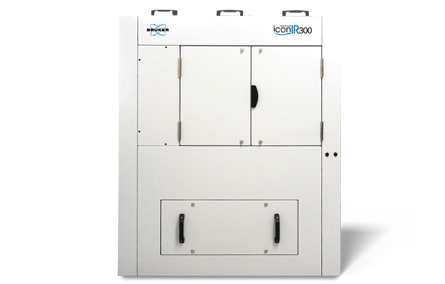
Dimension IconIR300
The Dimension IconIR300™ large-sample nanoIR system delivers rapid, high-accuracy nanoscale characterization for semiconductor applications, supporting a broad spectrum of material types and sample sizes up to 300 mm wafers. By combining proprietary photothermal IR spectroscopy with advanced AFM property mapping, IconIR300 enables automated wafer inspection and defect identification on samples that challenge conventional techniques. The system’s architecture supports rapid chemical imaging and quantitative analysis, extending AFM-IR capabilities to new semiconductor segments and materials. Integrated recipe-based measurement automation and robust data analysis software streamline workflows, ensuring reproducible, high-throughput measurements for process development, quality control, and production environments.
To learn more, continue reading, contact us, or see FAQs about this product.
Superior Nanoscale IR Spectroscopy and Chemical Imaging for the Semiconductor Industry
Only the Dimension IconIR300 system provides:
- Whole-wafer, non-destructive measurement of 200 mm and 300 mm wafers;
- Unambiguous identification of organic and inorganic nano-contaminants on semiconductor wafers and photomasks with data directly correlating to FTIR libraries;
- Non-destructive step-height measurement and nanoscale material property mapping; and
- Automated, recipe-based measurements and KLARF file support for user-friendly access to comprehensive data.
Whole-Wafer Measurement of 200 mm and 300 mm Wafers
Our patented, unique suite of AFM-IR modes and proprietary PeakForce Tapping® property mapping modes, together with IconIR300's large sample architecture, provide ultimate sample flexibility for the broadest range of semiconductor applications. IconIR300 delivers whole-wafer measurement of samples up to 300 mm in diameter in a wide range of thicknesses and material types, including:
- Both organic and inorganic samples;
- Patterned wafers;
- Bare wafers;
- Photomasks; and
- Data storage media wafers.
Additionally, Surface Sensitive AFM-IR mode enables IconIR300 to provide unique, reliable surface-sensitive chemical measurements of polymeric films deposited on semiconductor materials.
Push-Button AFM and AFM-IR Imaging Automation

Bruker’s AutoMET software on Dimension IconIR systems provides the only AFM-IR measurement automation capability on the market. It supports recipe-driven, push-button nanoscale chemical imaging, AFM imaging, and KLARF-based navigation. IR spectroscopy steps can also be inserted into automated imaging recipes.
AutoMET recipes allow the user to:
- Choose sites of interest
- Define measurements per site
- Set analyses per measurement
This level of automation is essential for routine industrial applications, from semiconductors to pharmaceuticals and polymers. Key benefits include:
- Increased throughput without repetitive manual imaging setup
- Consistent data acquisition from operators of any experience level
- Customizability for a large breadth of materials and analysis needs
Highest Performance Nanoscale IR Spectroscopy for Semiconductor Applications
Bruker is the innovator for photothermal AFM-IR-based nanoIR spectroscopy, the preferred technique for the nanoIR community.
Dimension IconIR300 delivers:
- Highly accurate, rich, detailed spectra with FT-IR correlation, achieving nanometer-level measurement of thin contaminants;
- A variety of advanced operational modes supporting the measurement of a wide range of samples for both industrial and academic users;
- Highest performance AFM-IR spectroscopy, the leading nanoIR mode in semiconductor applications; and
- Reliable surface-sensitive chemical measurements for polymeric films.

Highest Resolution Chemical Imaging On Wafers and Photomasks

The Dimension IconIR300’s industry-leading AFM performance and Bruker’s patented Tapping AFM-IR imaging together enhance the spatial resolution and sample accessibility of our nanoIR technology.
Dimension IconIR300 provides:
- <5 nm chemical spatial resolution for imaging over a broad range of sample types, including soft organic and inorganic contaminants;
- Consistent, reliable, and high-quality data; and
- AFM-IR technology for removing any and all mechanical artifacts, ensuring only true chemical composition is collected.
Dimension IconIR300 for Nanoscale Chemical and Surface Analysis
The Dimension IconIR300 is designed for nanoscale chemical identification and property mapping on full semiconductor wafers. By combining photothermal AFM‑IR spectroscopy with the industry‑leading Dimension Icon AFM platform, the system enables non‑destructive, whole‑wafer analysis with direct correlation to FTIR spectra. It is optimized for applications that require precise localization, high chemical sensitivity, and correlative nanoscale measurements across large samples.
Representative use cases include:
- Automated identification of organic and inorganic nano‑contaminants on 200 mm and 300 mm semiconductor wafers and photomasks
- Nanoscale defect characterization, linking composition with topography and material properties
- Chemical imaging of polymer residues, thin films, and patterned materials, including block copolymers and surface contaminants
- Surface‑sensitive nanoscale IR spectroscopy for polymeric and thin‑film materials
- Correlative chemical and material property mapping, combining nanoIR spectroscopy with PeakForce Tapping–based nanomechanical measurements
- Recipe‑based, high‑throughput wafer analysis, including defect navigation via KLARF file import and automated measurement workflows
LEARN MORE:
Chemical ID of Polystyrene Contaminants
In this real‑time demonstration, a Bruker nanoIR applications expert highlights the semiconductor‑focused capabilities of the Dimension IconIR300 through nanoscale defect identification on a full 300 mm wafer.
- Walks through IconIR300 hardware, including 300 mm wafer loading, alignment, navigation to defect sites, and tip engagement.
- Analyzes sample with 150 nm pitch structures and ~50 nm polystyrene particles, including particles on ridges and inside trenches.
- Shows strong agreement between IR images and topography, with zoom‑in views of nanoscale contaminants.
- Confirms that all particles share the same chemical identity, with intensity differences driven by particle size.
- Correlates nanoscale spectra with known FTIR signatures for material identification.


Frequently Asked Questions
Yes, this system is purpose-built for photothermal AFM-IR and property mapping on 200 mm and 300 mm wafers. It supports recipe automation and defect mapping for semiconductor workflows.
IconIR300 can detect and chemically identify both organic and inorganic nano-contaminants on wafers and photomasks. Its AFM-IR spectra can be directly correlated with FTIR reference libraries.
Yes. Dimension IconIR300 supports Bruker’s AutoMET® software and KLARF-based navigation. This enables user-defined automated nanoscale measurements at user-defined locations on wafers, grids, or arrays of multiple samples. IR spectroscopy steps can also be inserted into automated imaging recipes.
AutoMET® recipes allow the user to choose sites, then define measurements per site and analyses per measurement. This capability is essential for routine industrial applications, from semiconductors to pharmaceuticals and polymers.