Application Note: Characterizing Defectivity in SiC Wafers Using HRXRD Rocking Curves
Understanding Crystal Quality by Leveraging HRXRD
As the demand for SiC devices grows, so too does the need for effective characterization techniques to identify and quantify defects for assessing SiC wafer quality. This application describes how high-resolution X-ray diffraction (HRXRD) rocking curves can provide a highly sensitive, non-destructive, and comprehensive method for assessing defectivity in SiC wafers.
Contents include:
- Background information on the impact of defects on device performance and yield
- The role of HRXRD in SiC wafer quality control
- How to use Bruker HRXRD for high-throughput characterization of SiC wafers
KEYWORDS: High-Resolution X-Ray Diffraction; HRXRD; QCVelox; QC3; Delta-X; AN5201; Bruker; Application Note; SiC; Rocking Curves; Compound Semiconductor; Automation

Wafer Quality and Characterizing Defectivity in the Manufacturing Process
Defects in SiC wafers can significantly impact the reliability of devices. As industries, such as the automotive and aerospace industries, implement stricter regulations and standards for device quality, the ability to characterize the substrate properly becomes critical. Using HRXRD as part of a comprehensive quality control strategy ensures that wafers meet the required specifications early in the process, mitigating failure and improving yield.
Impact on device performance
The quality of SiC wafers directly influences the electrical, thermal, and mechanical properties of the resulting devices. Defects can degrade carrier mobility, increase leakage currents, and reduce breakdown voltages. High defect densities can lead to device failures, especially in high-stress environments typical of power electronics applications.
Impact on yield
Defective wafers can lead to significant losses during the fabrication process. Defects not only contribute to lower yields, but also necessitate expensive rework and extended testing. Identifying wafers and zones of wafers with high defectivity can reduce scrap rates and improve overall yield. By identifying defective wafers and zones early in the process, manufacturers can make informed decisions that enhance yield and reduce costs.
The Role of HRXRD in SiC Wafer Quality Control
HRXRD is a versatile, non-destructive analytical technique used to characterize SiC substrates with different orientations, sizes, doping levels, and polytypes—making it suitable for inline analysis of various SiC device fabrication processes. The technique provides valuable insights about structure, defect density, and overall quality of semiconductor wafers. It offers detailed information regarding crystalline structure, including lattice parameters, mosaicity, and strain.
This comprehensive analysis is essential for understanding how defects influence the electrical properties of SiC devices. By correlating HRXRD data with device performance metrics, manufacturers can establish a clear relationship between wafer quality and the reliability of end products, guiding production processes and improving yield rates.
The HRXRD omega scan, or rocking curve scan, is a well-known standard method for assessing SiC crystal quality because it is highly sensitive to various types of defects. Diffraction peak widths from these rocking curves are impacted by tilted or twisted grains and the presence of defects, such as dislocations, stacking faults, and point defects (shown in Figure 1). This technique enables manufacturers and researchers to quantify the density and distribution of these defects, allowing for a detailed assessment of wafer quality

Bruker HRXRD for Detailed and Rapid Wafer Quality Determination
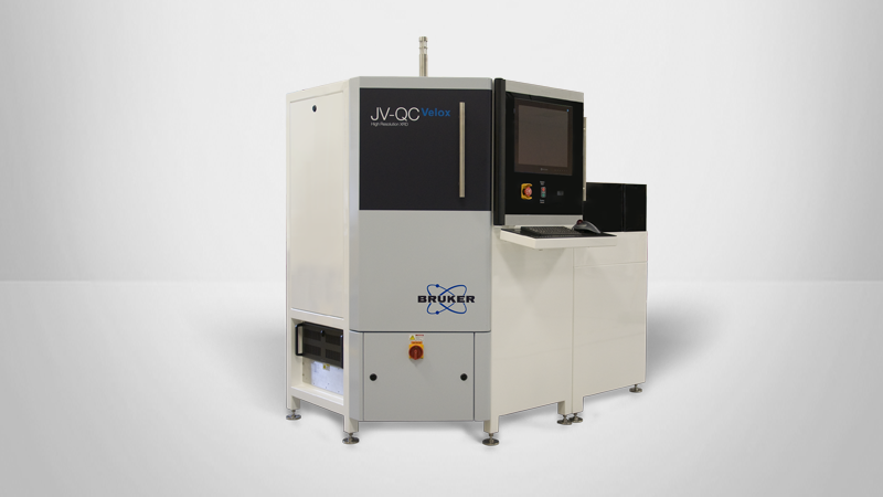
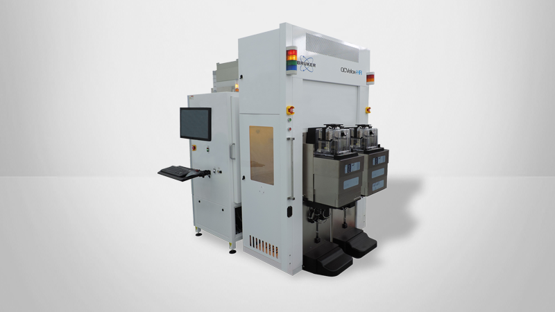
HRXRD is a powerful reference metrology technique used within silicon and compound semiconductor manufacturing. Bruker’s advanced HRXRD systems are sensitive to defectivity, enabling the characterization of the substrate and surface layers, a capability that is particularly beneficial for assessing the quality of epitaxial layers grown on SiC substrates. This is achieved by measuring a series of rocking curves, for both the substrate and for the grown films at offset positions, as shown in Figure 2. Using Bruker’s technology, these series of measurements and analysis can be automated and fully recipe-driven.
Bruker’s HRXRD systems can acquire data quickly, allowing for high-throughput characterization of SiC wafers. After loading and aligning a wafer on the system, an omega rocking curve can be collected in 15–20 seconds per site. Multiple sites can be collected for full mapping of a wafer’s defectivity. Plotting the peak full width half max (FWHM) across the wafer is common; however, it does not provide the complete picture.
With higher-quality materials, the FWHM is dominated by the bulk material, and defects lead to lower-intensity scatter affecting the width of the tails of the rocking curve. Therefore, FWxM, where x = 0.1, 0.01, etc. may be better indicators of sample quality. An example of complete 49-point wafer map across a 200 mm SiC wafer is shown in Figure 3. This technique is suitable for the characterization of all common semiconductor substrates, including SiC, Si, GaAs, InP, GaN, and others.

Understanding Crystal Quality by Leveraging HRXRD
As the semiconductor industry increasingly relies on SiC wafers for high-performance applications, effective characterization of wafer quality becomes essential. HRXRD rocking curves provide a highly sensitive, non-destructive, and comprehensive method for assessing defectivity in SiC wafers. Characterizing defectivity with HRXRD can enhance the understanding of failure mechanisms in SiC devices, leading to more reliable products and extended operational lifetimes. In R&D environments, HRXRD can be used to evaluate new growth techniques, materials, and process conditions, ensuring that advancements in SiC technology are based on high-quality substrates. By adopting this technology, manufacturers can improve defect detection, yield rates, and overall wafer quality, thus maintaining a competitive edge in the market.
Authors
- Peter Gin, Ph.D., Applications Manager, Bruker (peter.gin@bruker.com)
- Tamzin Lafford, Ph.D., Senior Applications Scientist, Bruker (tamzin.lafford@bruker.com)
©2025 Bruker Corporation. All rights reserved. All trademarks are the property of their respective companies. AN5201, Rev. A0.