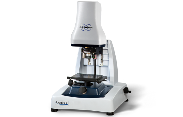
ContourX-100
具备最高性价比的 ContourX-100 光学轮廓仪为精确的、可重复的、非接触式表面测量树立了新基准。该系统占地面积小,所采用的简化方案融合了布鲁克几十年的专利白光干涉(WLI)创新技术,具有强大的二维/三维高分辨测量能力。新一代增强功能包括全新的 5MP 摄像头和更新平台,实现更多缝合功能,并新增一个测量模式 USI,提升了精加工表面、厚膜和摩擦学应用测量时的便捷性和灵活性。ContourX-100 堪称性价比最高的台式系统。
优异
Z向分辨率
提供不受放大率影响的一致的精准测量。
准确
计量值
简化设计,不影响测量功能。
友好
软件界面
提供对大量预编程过滤器和分析程序的直接调用。
卓越计量能力
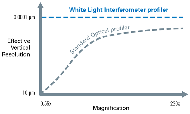
白光干涉所有物镜均提供恒定的最佳垂直分辨率。
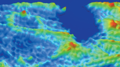
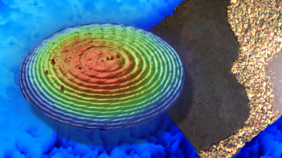
ContourX-100 轮廓仪是布鲁克 40 多年来在非接触式表面计量、表征和成像领域专有光学创新和行业领导力的结晶。该系统利用三维 WLI 和二维成像技术,一次采集可执行多次分析。ContourX-100 在反射率 0.05% 到 100% 的所有表面情况下都能发挥稳定性能。
独一无二的价值和分析
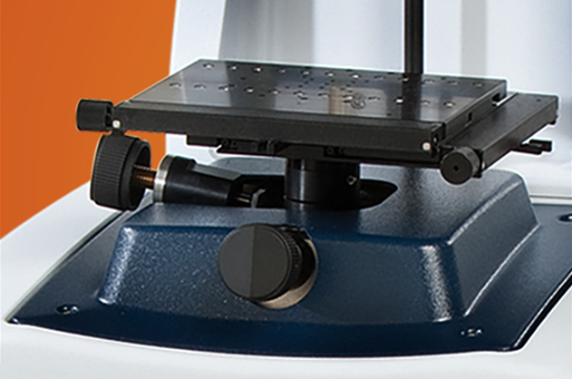
ContourX-100 手动平台。
ContourX-100 台式可执行数千种自定义分析,并采用布鲁克简单而强大的 VisionXpress 和 Vision64 用户界面,提升了实验室和工厂的生产效率。软硬件的完美结合,实现简便操作下的高效率光学性能,全面超越同类计量技术。