Surface Characterization of Semiconductors: An Overview, from Topography to Advanced Physical Properties
Learn about Bruker’s high-performance metrology techniques for the nanometer-scale surface characterization of semiconductor materials and devices
Introduction to Bruker's Portfolio of Solutions for Semiconductor Characterization
PRESENTATION HIGHLIGHTS:
- [00:01:28] Webinar Agenda
Bruker Semiconductor Products Portfolio
- [00:04:15] 3D Optical and Stylus Metrology
- [00:04:55] Tribology and Mechanical Testing
- [00:05:24] NanoIndentation
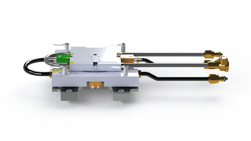
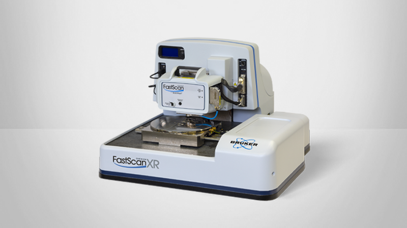
- [00:05:58] Atomic Force Microscopy
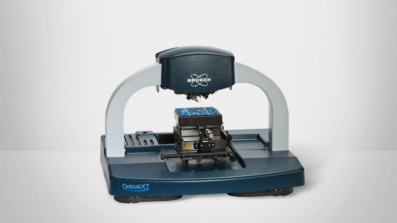
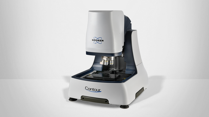
Semiconductor M3D Metrology Using Optical and Stylus Profiling
PRESENTATION HIGHLIGHTS:
- [00:00:00] Introduction to Stylus and Optical Profilometry
Stylus Profiler Applications
- [00:05:05] Step Height and Thin Film
- [00:07:21] Bow and Thin Film Stress
Optical Profiler Applications
- [00:14:16] Packaging & Fan-Out
- [00:31:02] CMP Optimization & Die Flatness
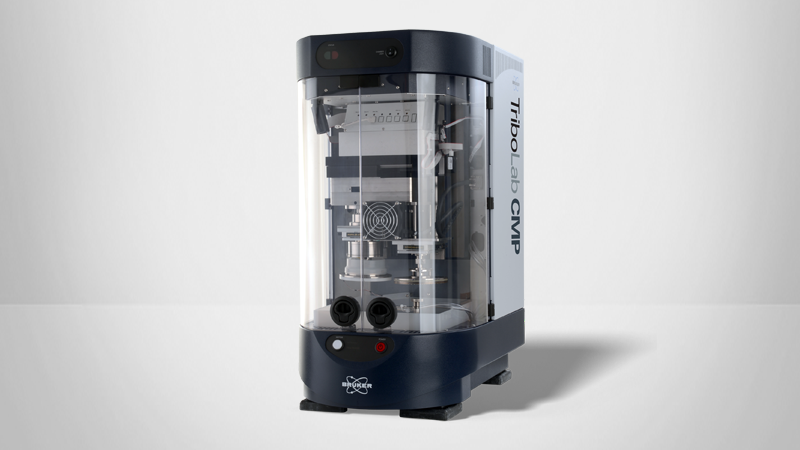
CMP Tribology
PRESENTATION HIGHLIGHTS:
- [00:00:00] Introduction to Chemical-Mechanical Polishing for semiconductors
- [00:01:43] Fundamentals of Chemical-Mechanical Polishing
- [00:02:55] Important Factors in Chemical-Mechanical Polishing
- [00:04:10] Bruker Tribolab CMP Tester
- [00:09:17] CMP Application Examples
- [00:14:51] Summary
Mechanical Characterization of Semiconductor Samples and Devices
PRESENTATION HIGHLIGHTS:
- [00:00:24] Nanoindentation Basics
- [00:02:23] Mechanical Testing Landscape
- [00:05:20] Expansion of TSV - in situ observation
- [00:07:27] Mechanical Property Testing
- [00:13:31] Advanced Testing
- [00:16:41] Bruker's Hysitron Nanoindenter Product Portfolio
Highest Resolution 3D Metrology and Advanced Physical Property Characterization of Semiconductor Samples and Devices
PRESENTATION HIGHLIGHTS:
High-Resolution Topography
- [00:01:08] Principles of AFM
- [00:02:20] Surface Topography Imaging
- [00:05:01] Dimensional Metrology
- [00:10:11] Defect Review/inspection
- [00:13:11] Practical Demonstration
Beyond Topography
- [00:20:06] Nano-Electrical
- [00:26:06] Nano-Mechanical
- [00:29:54] Nano-Chemical