

Nanophoton Series Microscopes
Meet the RAMANfamily
The RAMANfamily combines precision optics with galvanometer scanning to match your research needs—whether you're exploring the nanoscale point by point or analyzing entire wafers with area imaging. Discover the unique strengths of RAMANtouch, RAMANwalk, and RAMANdrive. Three instruments. One game-changing technology.
The Engine Behind Nanophoton’s Speed: Galvo Scanning
Galvanometer scanning redefines how Raman microscopes interact with samples. Faster, more stable, and more versatile than stage- or table-based movement, Nanophoton systems combine both methods for the best of both worlds.
In Nanophoton systems, a galvanometer mirror precisely steers a line-shaped laser beam across the sample. This laser line excites Raman signals along a full cross-section of the sample in a single pass.
The emitted Raman light passes through a confocal slit, which ensures spatial filtering and optical sectioning, then enters a spectrograph that disperses the light by wavelength. The dispersed signal is captured by a CCD detector with a 2D pixel array.

Galvo Scanning is faster.
Galvanometer scanning uses ultra-responsive mirrors, controlled by electromagnetic actuators, to steer the laser beam with precision. Rather than moving the entire table/stage, the laser is directed optically at high-speed across the sample surface without physical contact or inertia.
Imagine a spotlight sweeping across a stage to follow the actors—smooth and precise. Now imagine moving the entire stage under a fixed light. Instantly, the advantages become clear.
Nanophoton combines it with table scanning.
Traditional Raman systems rely on table scanning, where the sample is moved step-by-step under a stationary laser beam. This mechanical method introduces delays, potential vibration, and limits imaging flexibility.
And because Nanophoton systems combine galvanometer and motorized table scanning, you get the best of both: fast optical beam movement to capture fine details in the field-of-view much faster, and stage movement for large areas.
There are three different laser modes.
In Nanophoton Raman microscopes, galvanometer mirrors control the laser’s path across X- and Y-axes, enabling:
- Point Mode
Focused spectra at precise positions - Line Mode
High-throughput linear scans across sample - AreaFlashTM Mode
Capture large Areas in a single exposure
| Galvanometer Scanning | Traditional Table Scanning | |
| Speed | Millisecond-level laser movement | Slower mechanical positioning |
| Vibration / Drift | None (no sample movement) | Potential vibration and drift |
| Scan Modes | Point, Line, Area | Point, 3D |
| Precision | Sub-micron laser positioning | Limited by stage mechanics |
| Flexibility | Combines with stage scanning when needed | Stage-only in most systems |
The Story of Nanophoton
History of Nanophoton
Nanophoton’s story began in 2003 as a venture from Osaka University led by Professor Satoshi Kawata, a pioneer in photonics and microscopy. The young company set out with the bold mission to create “A Scientist’s Company.” From the very beginning and continuing to this day, Nanophoton’s engineers and sales staff have worked closely with universities and industrial labs to develop unique and original products.
In 2005, Nanophoton delivered breakthrough technology almost immediately by introducing the RAMAN-11 – the world's first laser-scanning confocal Raman microscope. This breakthrough was quickly recognized, as rapid market success validated Nanophoton’s technology and built trust among scientists and companies in Japan.
By 2006, Nanophoton had won the Japan Venture Award, and in 2007, the company leader Professor Kawata was honored with the Emperor’s Purple Ribbon Medal, a prestigious national award in Japan, for his remarkable professional accomplishments. Over the next decade, the company continued releasing new systems, quietly but steadily growing its reputation in both academia and industry.
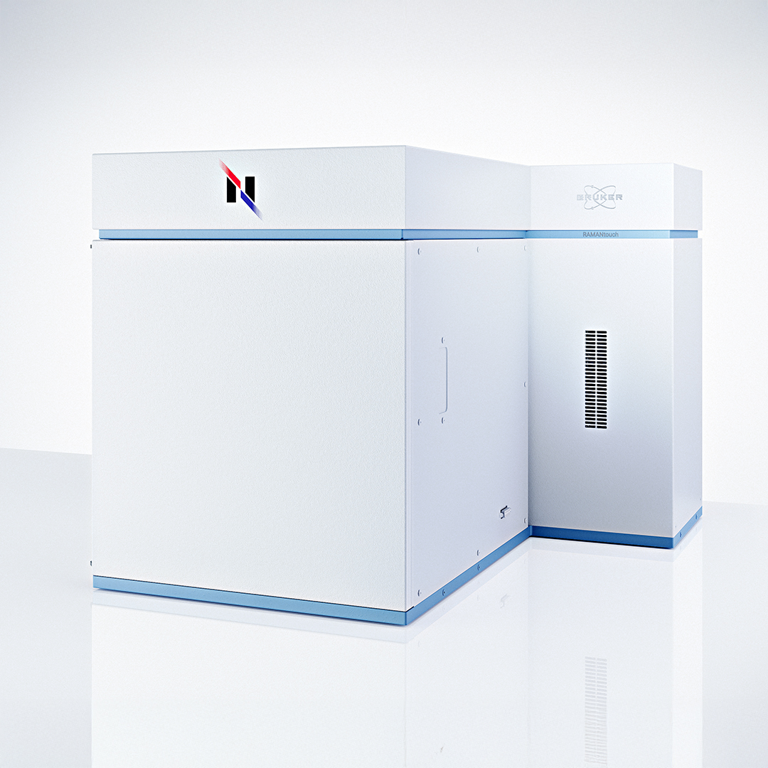
In 2011, Nanophoton released the first generation of its flagship confocal Raman microscope, the RAMANtouch, which featured its most advanced imaging design to date. A patented line-shaped laser illumination combined with a fast galvanometer scanner, allowing the capture of hundreds of spectra simultaneously in a single scan. This design made imaging extraordinarily fast and reduced measurement time by a factor of several hundred.
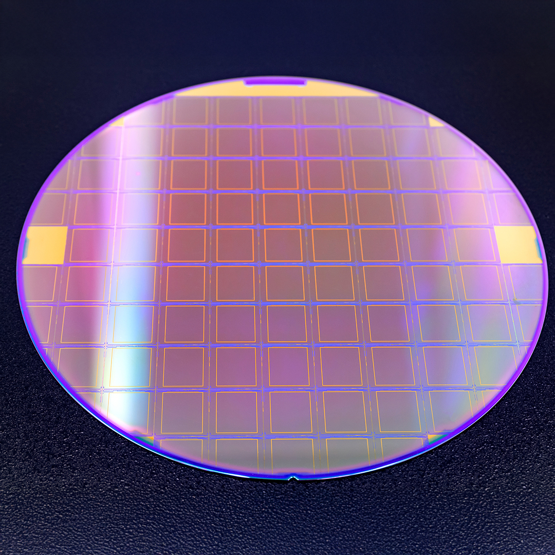
This allowed researchers to acquire large-area chemical maps of a sample in minutes rather than hours, giving them rapid, high-resolution data. Building on this success and continually refining its technology, more specialized instruments followed: in 2016, the RAMANdrive for 300 mm semiconductor wafer inspection was launched, and in 2018, a deep-UV Raman microscope (RAMANtouch vioLa) for advanced photonics research was introduced.
Nanophoton Today
Today, researchers in materials science, electronics, batteries, polymers, and pharmaceuticals use Nanophoton microscopes for tasks such as plotting active ingredients and excipients in pharmaceutical tablets, analyzing 2D materials, and even exploring the secrets behind tasty chocolate by imaging its fat content. The company’s focus on user-driven solutions and patented technology has earned it strong support from customers, especially in Japan and Korea.
Many of these customers are global science and industry leaders. Companies such as Sony, Hitachi, and Panasonic, as well as Japan’s energy giant ENEOS, employ Nanophoton microscopes for product development and quality control. In advanced materials and device innovation, Samsung Electronics relies on Nanophoton for its imaging needs. LG Chem, a leader in battery and energy storage technology, uses Nanophoton’s systems to analyze materials critical to the next generation of energy solutions.
In the chemical and pharmaceutical fields, FUJIFILM integrates Nanophoton’s imaging technologies into its polymer materials research. Semiconductor manufacturing leaders such as SK Materials, SK On, and FST utilize Nanophoton’s solutions for their processes. Even global consumer tech innovator Dyson and Korean food and bioscience company Daesang turn to Nanophoton for their specialized research requirements. This diverse customer base testifies to the broad acceptance and trust Nanophoton has earned across sectors.
Beyond industry, Nanophoton’s instruments have become indispensable to many of Asia’s top academic and research institutions. Prestigious universities such as The University of Tokyo, Kyoto University, Osaka University, and Tohoku University, along with national research institutions like RIKEN, collaborate with Nanophoton on pioneering studies in materials science, chemistry, and life sciences. These collaborations have resulted in thousands of published journal papers.
A New Chapter with Bruker
After two decades of steady growth, product innovation, and trusted service in Japan and Asia, Nanophoton took a strategic step in 2024 by merging with Bruker. Today, as "Nanophoton – a Bruker Company", the combined strengths allow customers worldwide to benefit from the unmatched speed, sensitivity, and spatial resolution of Nanophoton’s confocal Raman microscopes, now backed by Bruker’s extensive global support network.
The famed instruments, acclaimed by leading corporations and top universities across Japan and Asia, are now available on an even broader scale.
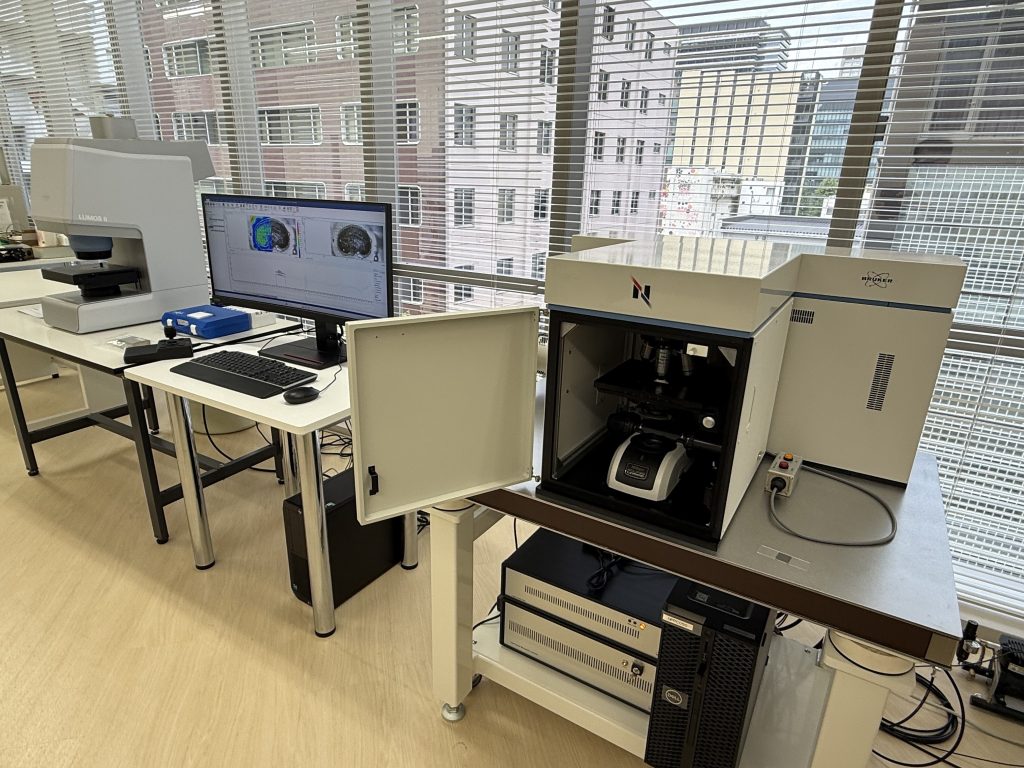
The IR and Raman Imaging Center
On May 8, 2025, the Bruker–Nanophoton Raman-IR Imaging Center officially opened in Toranomon, Tokyo. Formerly Nanophoton’s Tokyo showroom, the renovated and expanded facility now showcases state-of-the-art Raman and infrared microscopes — likely the only place worldwide where both technologies can be experienced side by side for advanced materials research.

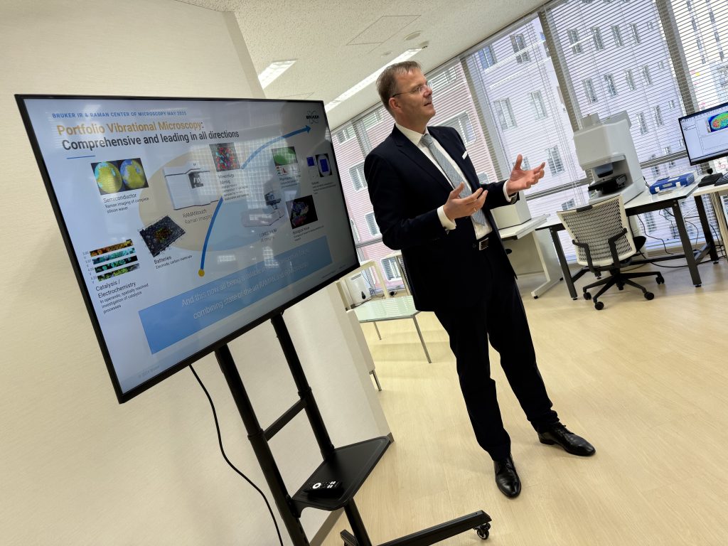
The opening ceremony featured remarks from Andreas Kamlowski (President, Bruker Optics), Christian Werner (VP Global Sales, Bruker Optics), Shigeru Shimada (Head of Bruker Japan Optics), and Professor Satoshi Kawata, Nanophoton’s founder and Chief Scientific Officer. Presentations followed from Taikan Minamoto on Nanophoton’s Raman microscopes and from Shimada on Bruker’s infrared systems. Live demonstrations and a networking reception completed the event.
The center symbolizes the merger of Nanophoton and Bruker, bringing together two pioneers in Raman and infrared microscopy. Professor Kawata emphasized that scientific and organizational barriers — between disciplines such as physics, chemistry, and engineering, or between corporate silos — often hinder innovation. The collaboration aims to break down these walls and foster a more integrated, transdisciplinary approach to research and development.
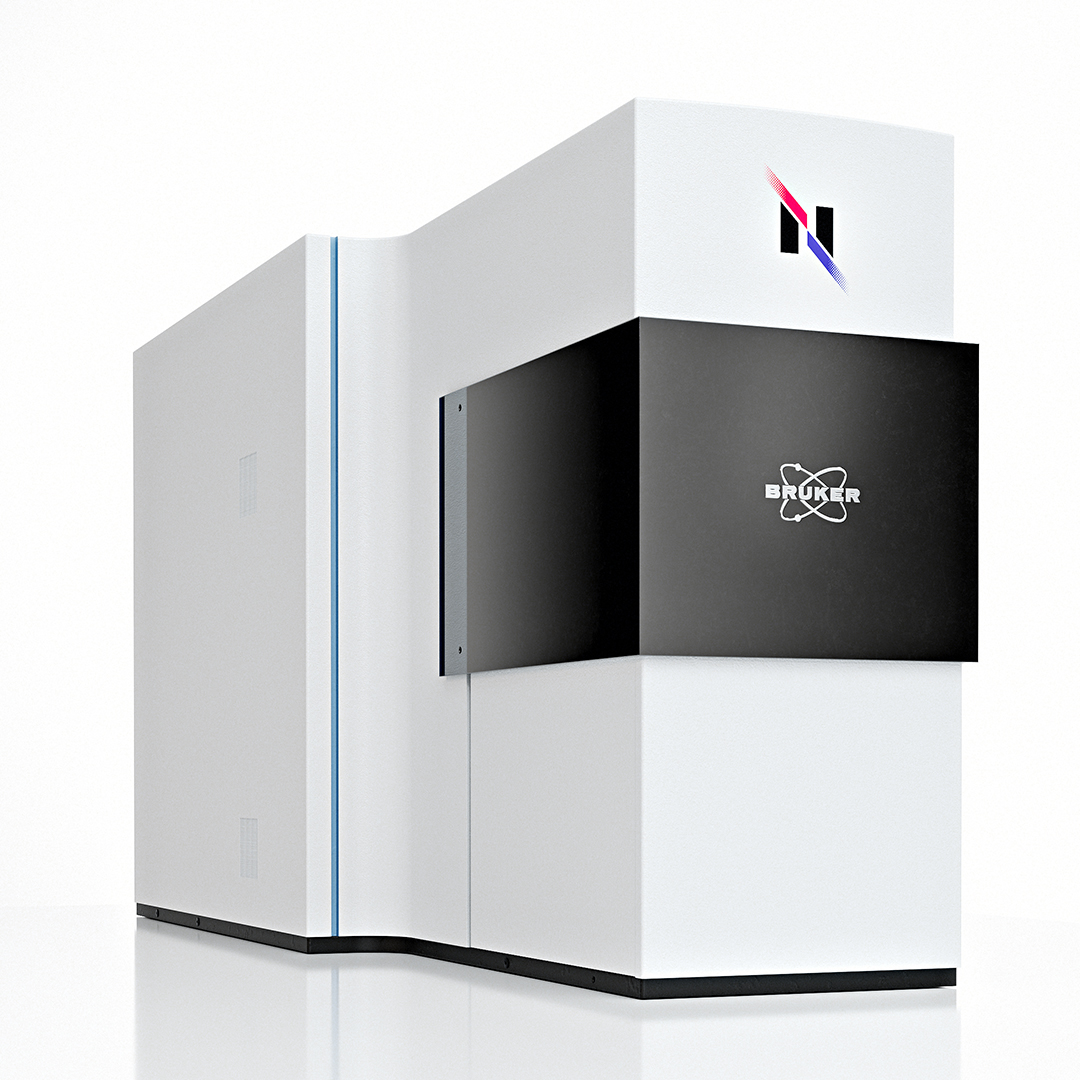
The merger was described as a partnership of equals: while Nanophoton is now legally part of Bruker, its brand, logo, and product names remain unchanged. A new design element — a subtle Bruker-blue line added to Nanophoton’s signature white instruments — symbolizes this union.
With the launch of the Raman-IR Imaging Center, Bruker and Nanophoton seek to provide researchers with an open, collaborative space and to accelerate innovation in advanced materials science worldwide.


