
EDS of semiconductor lamellae in SEM (T-SEM) and STEM
Quantitative Element Mapping of Electron-Transparent Samples
The continuous miniaturization of semiconductor structures requires their understanding on the nanoscale to ensure suitable design and failure analysis. Many investigations need expensive measurement times on high-end transmission electron microscopes as well as complex specimen preparation and specimen transfer routines.
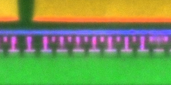
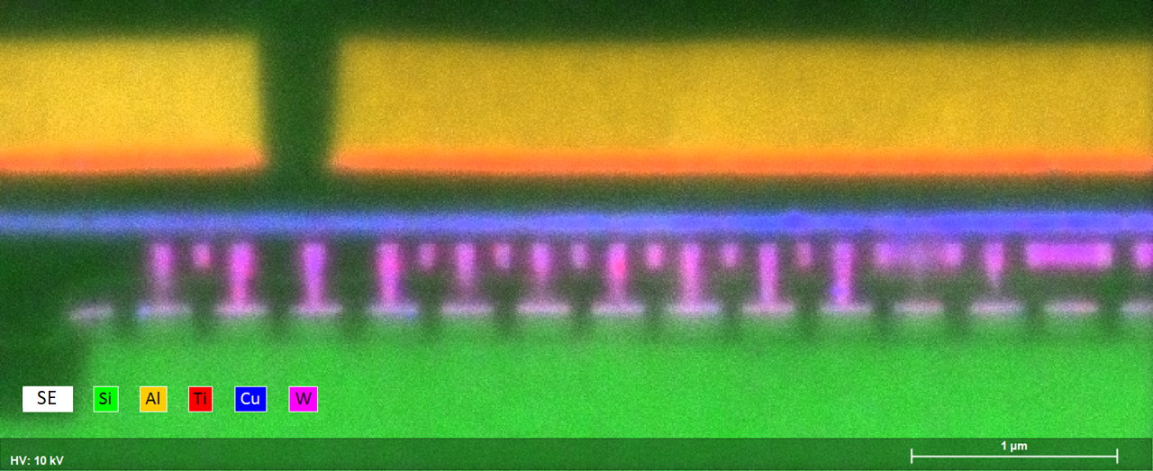
We show options to evaluate the element distribution in electron transparent samples, e.g. FIB lamellae, using energy dispersive X-ray spectroscopy not only in TEM, but also in SEM (Fig.1) or during FIB. Single, multiple, and annular Bruker XFlash® detectors are available for fast data acquisition. Efficient approaches for quantitative EDS of electron transparent specimens in SEM (so-called T-SEM) and in STEM are presented.
Furthermore, EDS is correlated with other analysis techniques, such as non-destructive micro X-ray fluorescence analysis (micro-XRF) using the Bruker M4 TORNADO and Transmission Kikuchi Diffraction (TKD) using electron transparent specimens in SEM.
Who Should Attend?
- Scientists and application scientist from semiconductor fabs and labs
- Academic staff and students interested in FIB, specimen preparation, SEM- and TEM-EDS, and related analysis techniques for element and structure analysis
Speakers

Dr. Meiken Falke
Global Product Manager EDS/TEM, Bruker Nano Analytics

Max Patzschke
Application Scientist EDS, Bruker Nano Analytics

Dr. Purvesh Soni
Sr. Applications Scientist EDS, Bruker Electron Microscope Analyzers

Watch this Webinar On-Demand
Please enter your details below to gain on-demand access to this webinar.