Additive Manufacturing
Solutions and Support for Industry-Leading Manufacturing Processes
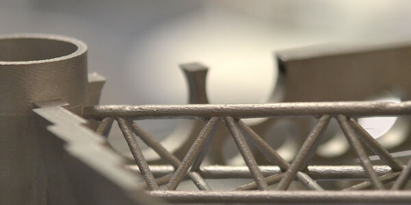
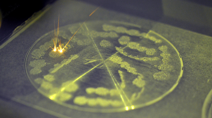
Automotive and aerospace companies are in a constant race to increase energy efficiency and design flexibility, lower production and service costs and reduce manufacturing cycle time while ensuring the reliability and safety of their products. For many of these companies, additive manufacturing (AM) looks like the solution to all of these market demands. Most rapidly emerging and popular AM processes for metals are based on a powder bed: a metallic powder is formed into a solid state through melting or sintering. Common melting techniques consist of scanning a laser (Direct Laser Selective Melting, DLSM) or electron beam (Electron Beam Melting - EBM) across subsequent layers of metal powder in a “printer’s” powder bed to build up a final, finished AM part. The technique is also known as powder bed fusion or LPBF. Another AM technology is vat photopolymerization making up close to 50% of the material use in AM. Vat Photopolymerization is a process in which liquid photopolymer in a vat is selectively cured by light-activated polymerization.
However, many companies find that the move from prototyping to production with AM is challenging. To get defect-free, repeatable results requires process characterization and QA/QC controls that are unique to AM. Bruker has unmatched experience and breadth of solutions to help maximize AM Profits.
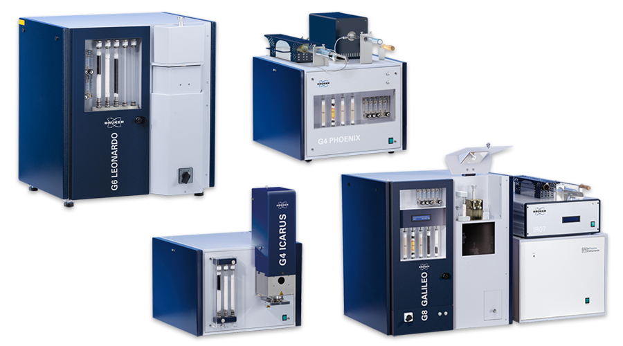
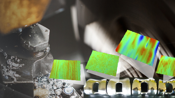
Correctly specifying and monitoring the chemical and mechanical properties of raw materials used in the AM process is absolutely critical. Inclusions, voids, porosity variation as well as changes is mechanical properties (hardness, brittleness) can result from improper alloy/mixture use and contamination of incoming, stored and recycled powders.
The AM printing process itself, if not properly characterized, can also be a source of a wide range of defects. An optimum balance needs to be found between scanning speed, laser or electron beam power, beam incident angle, thermal load on the surrounding powder bed, powder particle size, and bed thickness. For vat photopolymerization, not only the mixture composition but also the curing kinetics of the photopolymer is of great importance for the result. To characterize the AM process and monitor witness samples during production and after finishing steps (heat treatment-HIP, milling and grinding/polishing, UV curing), Bruker offers an unmatched suite of products for dimensional, chemical and mechanical testing and analysis.