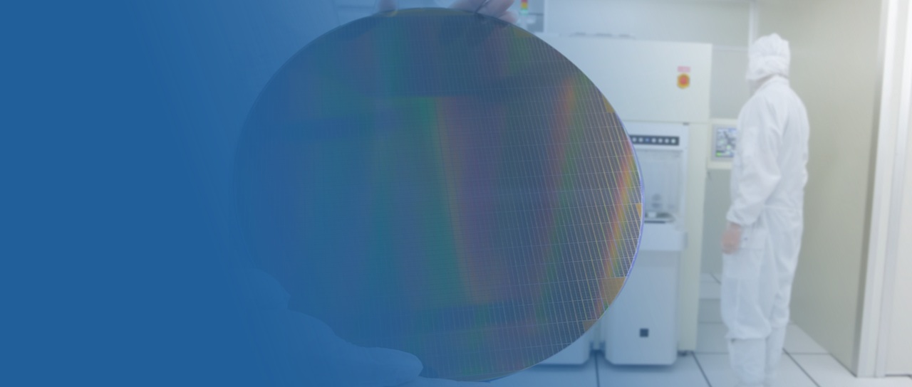
Mask Repair and Wafer Cleaning
Production-Enhancing Technology
Bruker provides production-enhancing photomask repair and cryogenic dry cleaning technologies for advanced semiconductor manufacturing.
Our photomask repair solutions address critical production challenges associated with controlling pattern defects on high-end photomasks, including quartz bumps on alternating phase shift masks, carbon patch trimming, multi-level materials, foreign materials, persistent unknown particles, and repairs within tight lines and spaces. Complementing these capabilities, cryogenic CO₂ cleaning systems remove contaminants and residues from wafers, photomasks, and electronic devices using a fast, non-destructive, waste- and residue-free process that eliminates corrosion and staining.
Together, these technologies help manufacturers maintain the quality and cleanliness standards required for advanced semiconductor production.
Find the Right Solution for You
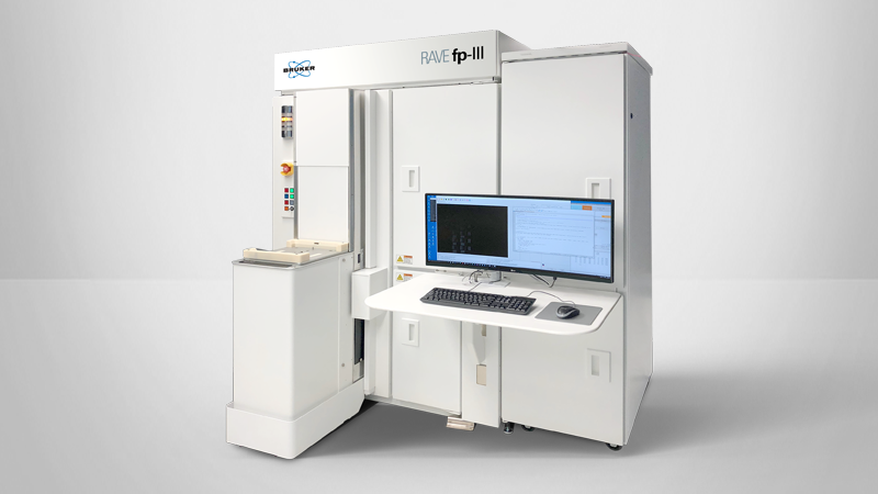
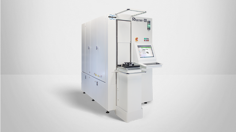
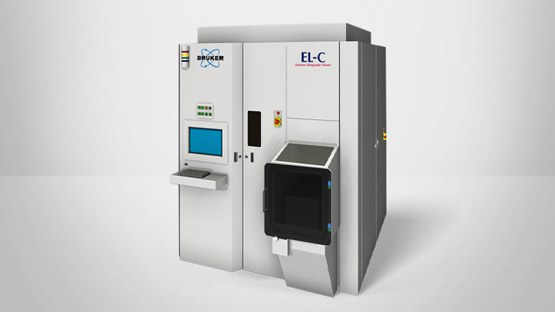
Photomask Repair Systems
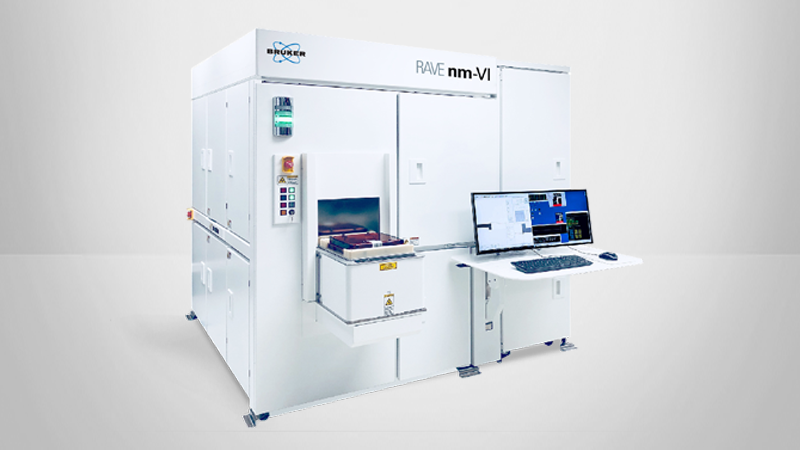
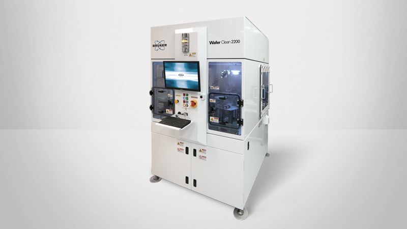
Mask and Wafer Cleaning Systems
Defect and Contamination Control Technologies for Semiconductor Manufacturing
Bruker’s photomask repair and cryogenic CO₂ cleaning solutions help semiconductor manufacturers address critical production challenges associated with pattern defects, particles, residues, corrosion, and staining. From high-end photomask repair to photomask and wafer cleaning, these technologies support the quality and cleanliness requirements of advanced manufacturing environments.
To learn more, contact us to discuss your measurement requirements, find out about the systems best-suited for your application, discuss options for system specialization, or request a quote based on your specific needs.

Photomask Defect Repair
Address critical production challenges associated with controlling pattern defects on high-end photomasks, including quartz bumps on alternating phase shift masks, carbon patch trimming, multi-level materials, foreign materials, persistent unknown particles, and precision repairs within tight lines and spaces.
- High-end, complex photomask repair
- Precision repairs within tight lines and spaces

Particle, Residue, & Surface Contamination Removal
Remove contaminants and residues from wafers and electronic devices using dry cryogenic CO₂ cleaning technology that is extremely fast, environmentally friendly, cost-effective, non-destructive, waste- and residue-free, and eliminates corrosion and staining.
- Removal of corrosion and staining
- Mask particle removal and 3D metrology
Frequently Asked Questions
Frequently Asked Questions About Photomask Repair
Bruker's photomask repair solutions are designed to address critical production challenges associated with controlling pattern defects on high-end photomasks, including quartz bumps on alternating phase shift masks, carbon patch trimming, multi-level materials, foreign materials, persistent unknown particles, and repairs within tight lines and spaces.
The control of pattern defects becomes increasingly important as feature sizes shrink and mask complexity increases. Bruker's repair technologies are designed to support advanced photomask production, including multi-patterning and EUV lithography environments.
Bruker's photomask repair portfolio includes femto-pulse laser repair, AFM-guided nanomachining, haze removal, and AFM-based defect review and particle removal technologies for advanced mask manufacturing environments.
Bruker solutions support high-end, complex photomask repair, precision repairs within tight lines and spaces, mask particle removal, and photomask defect review and metrology.
Frequently Asked Questions About Mask and Wafer Cleaning
Cryogenic CO₂ cleaning offers a fast, environmentally friendly method for removing contaminants and residues from photomasks, wafers, and electronic devices. The process is cost-effective, non-destructive, waste- and residue-free, and eliminates corrosion and staining associated with conventional cleaning approaches.
Our customers benefit from many inherent aspects of the technology and the perfected, patented features of Bruker's equipment. Our cryo dry cleaning systems deliver on a low cost of ownership with:
- Superior cleaning performance using our patented nozzle design
- Proven 24/7 production performance for high-demand applications
- High throughputs ensuring high capital utilization
- Compact system design requiring minimal cleanroom space
- Yield improvements not seen with standard wet or plasma cleaning processes
Bruker's cryogenic CO₂ cleaning systems are used to remove contaminants, particles, and residues from photomasks, wafers, and electronic devices across a broad range of semiconductor applications.
Cryogenic CO₂ cleaning combines contamination removal with a non-destructive, non-aqueous process that is extremely fast, environmentally friendly, cost-effective, and free of waste and residues. The technology also eliminates corrosion and staining while supporting demanding semiconductor cleanliness requirements.
As the leading innovator of dry CO2 technology, Bruker sets the standard for quality dry process cleaning. The company currently holds over 25 U.S. and International patents in many areas of cryogenic CO2 cleaning. This innovation has been the standard in production cryogenic CO2 cleaning for over 30 years.
Our state of the art applications lab in Delray Beach, FL provides a location where our global customer base can come to develop new cleaning techniques or optimize their existing processes.
To learn more about how Cryogenic CO2 cleaning technology can resolve your most difficult contamination problems, please contact us for more information or schedule a demonstration.
Get Expert Answers
Ask us a question, request more information, or get in touch with a Bruker sales representative.