
XFlash® 7 - EDS Detector Series
Energy Dispersive Spectrometry for SEM, FIB-SEM and EPMA
XFlash® 7 - The EDS Detector for Scanning Electron Microscopy
- Achieve unmatched analysis speed.
- Quantify the most complex data using the most comprehensive atomic database incl. K, L, M and N lines.
- Maximize your sample throughput with the best available geometric collection efficiency of the generated X-rays.

Element Analysis in Transmission Electron Microscopy on the Nanometer Scale

XFlash® 7T - The EDS Detector for TEM, STEM and T-SEM
- Identify and quantify all present elements unequivocally supported by higher energy element lines.
- Succeed in TEM, STEM and T-SEM with easy-to-use powerful quantification procedures based on theoretical and experimental Cliff-Lorimer factors, as well as Zeta-factor interpolation.
- Map periodic structures (atoms, layers) with high stability and as comfortably as non-periodic features supported by dedicated drift correction routines.
Applications of the XFlash® 7 EDS Detector Series
The XFlash® 7 EDS detector series delivers high-performance elemental analysis to scanning electron microscopists across a wide range of applications.
For SEM EDS the XFlash® 7 series offers unmatched analysis speed and precision, enabling fast and accurate mapping even of complex samples. ESPRIT LiveMap facilitates the quick identification and localization of regions of interest for further in-depth analysis.
For TEM, STEM and T-SEM EDS the XFlash® 7T series supports high-resolution quantification down to the atomic scale, with advanced drift correction and quantification models tailored for nanoscale analysis.
Learn more about applications of XFlash® 7 detectors using the links below.

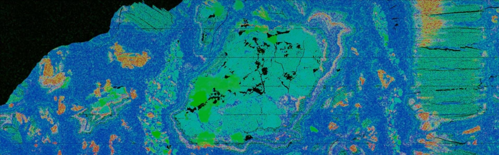
High input count rate EDS map of a failed welding seam of zirconium and stainless steel.