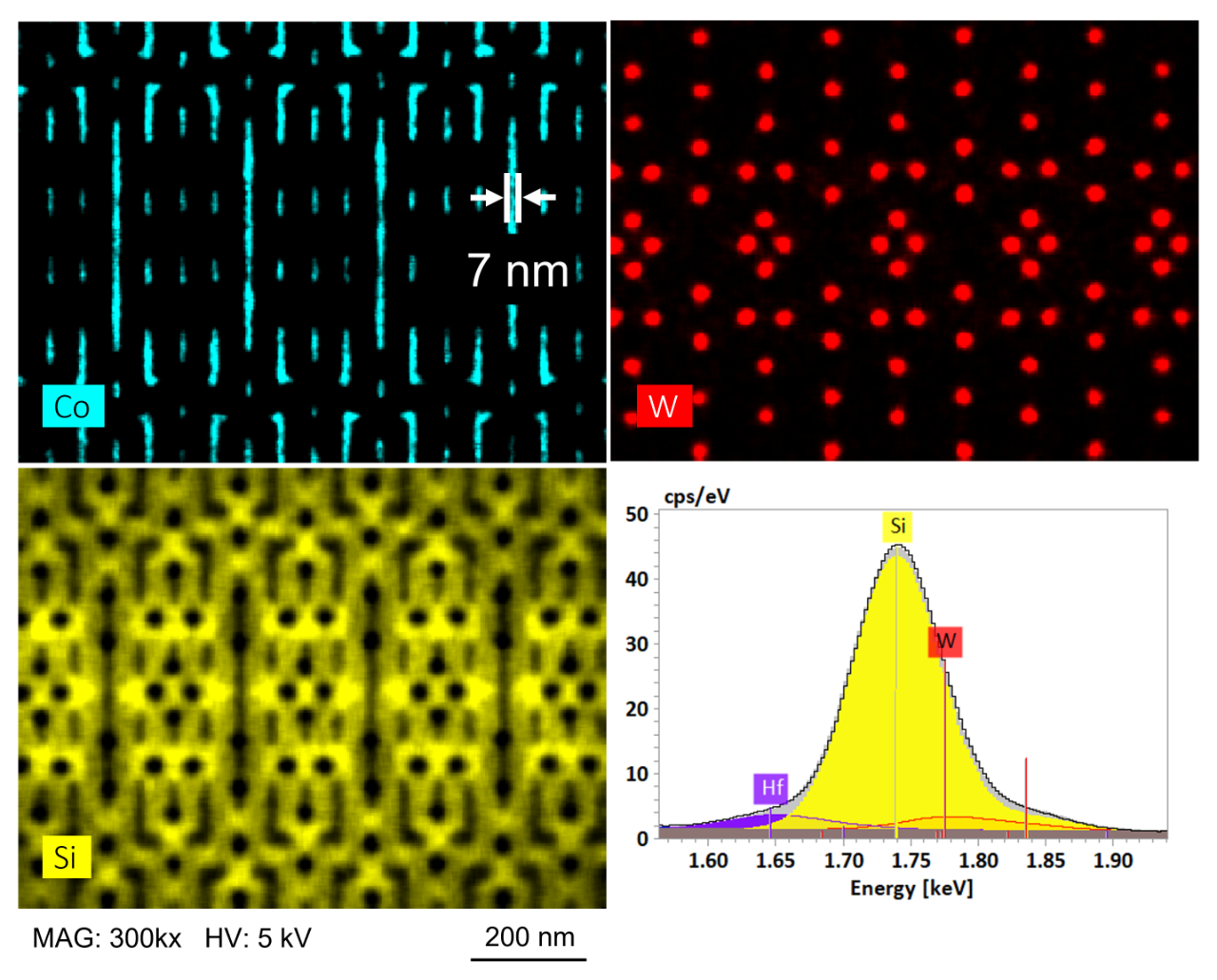
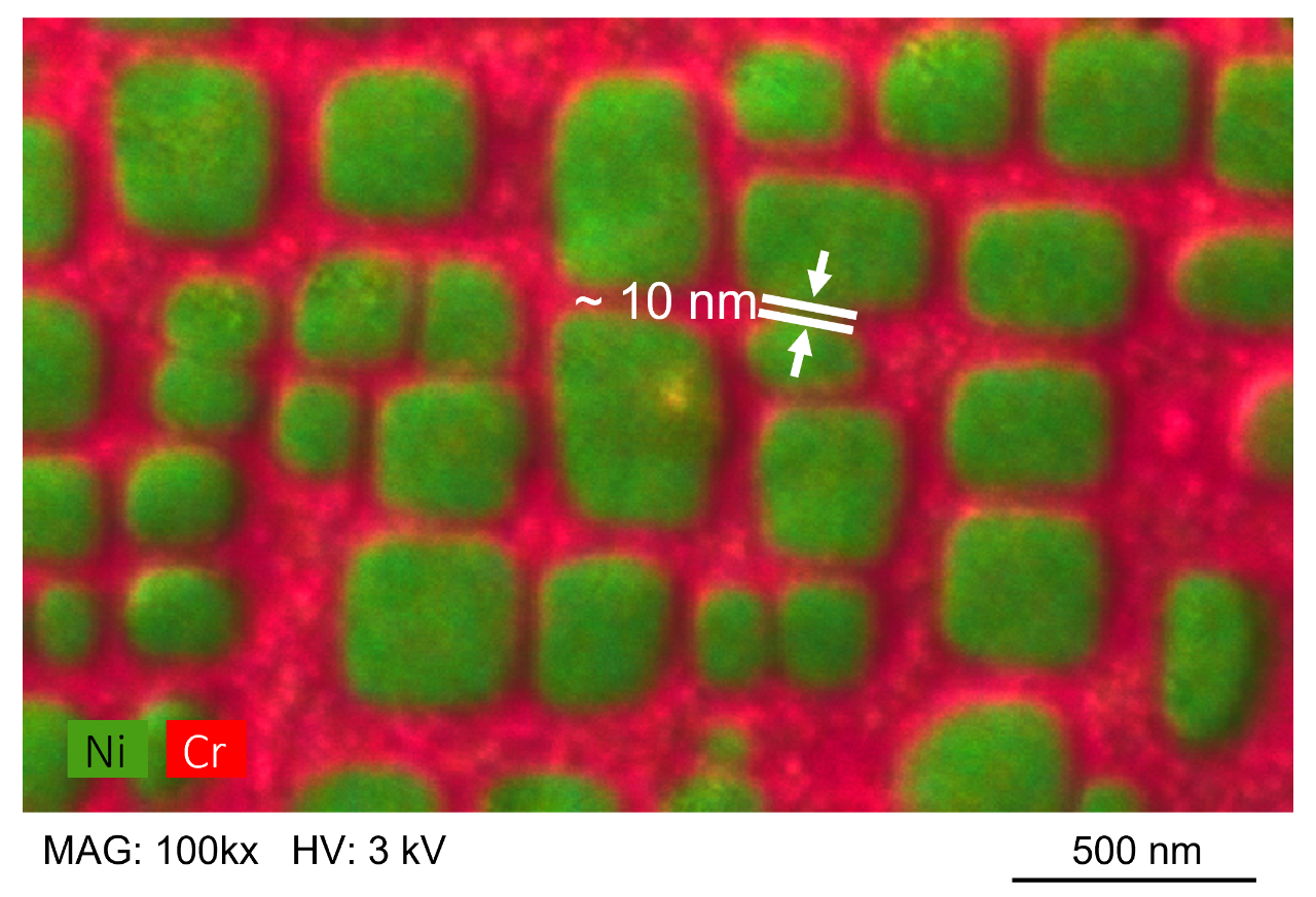
Achieving sub-10 nm EDS Spatial Resolution on Bulk Specimen in SEM
Measurements at High Spatial Resolution
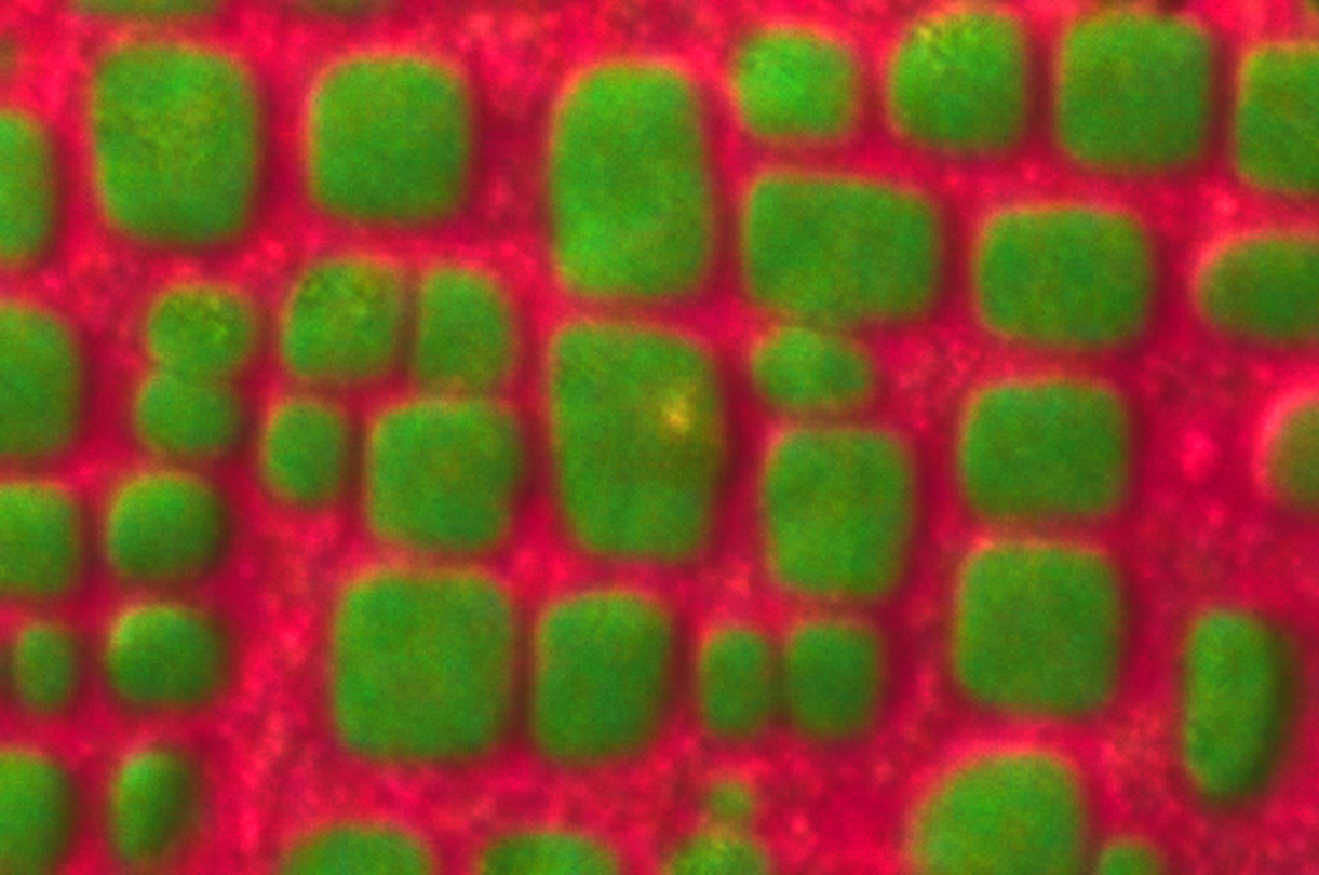
Chemical mapping of nanoscale features in bulk samples is known to be very challenging since it requires achieving simultaneous high spatial resolution imaging and spectroscopic analysis. The typical alternative is chemical mapping on electron transparent samples in STEM.
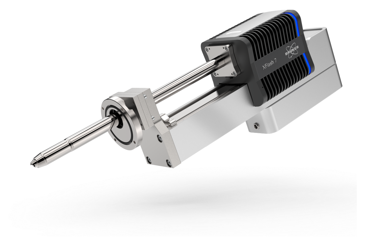
The newly launched Bruker XFlash® 7 EDS detectors have the best solid angle and highest pulse processing speeds ensuring the highest collection efficiency and high sensitivity. This combination is ideal for measurements at high spatial resolution because it provides excellent output count rates at low probe currents.
In this webinar, we demonstrate examples of bulk semiconductor and aerospace materials with challenging element combinations, where sub-10 nm EDS-spatial resolution are achieved using low and high kVs. We also discuss the common challenges for acquiring high spatial resolution EDS data on bulk materials in SEM and show you how to maximize the analytical capabilities of your SEM.
If you want to learn more about how to enhance your EDS make sure to view the other webinars available in our XFlash® 7 series:
Speakers

Dr. Purvesh Soni
Sr. Applications Scientist EDS, Bruker Electron Microscope Analyzers

Dr. Igor Németh
Application Scientist EDS, Bruker Nano Analytics
* The On-Demand registration form is optimized to work with the browser Google Chrome.
Watch this Webinar On-Demand
Please enter your details below to gain on-demand access to this webinar.