AFM Imaging and Beyond: A Practical Guide to AFM Modes for Materials Research
Learn from the leaders in AFM mode innovation
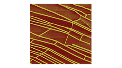
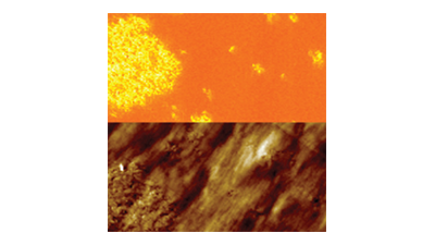
AFM Modes 101
PRESENTATION HIGHLIGHTS:
- [00:00:00] General Imaging Modes
- [00:01:12] Derivative Modes, Optimized Probes, & Relevant Environmental Control
- [00:04:21] Mechanical Applications
- [00:05:31] Electrical Applications
- [00:06:21] Fabrication Applications
- [00:07:30] Chemical Applications
- [00:09:00] Electro-Chemical Applications
- [00:10:06] Thermal Applications
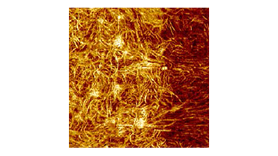
Case Study: Polymer Research
PRESENTATION HIGHLIGHTS:
- [00:00:00] Phase Imaging with TappingMode
- [00:02:46] PeakForce QNM
- [00:04:38] AFM-nDMA
- [00:06:46] AFM-IR
- [00:08:36] Temperature Studies with Heater/Cooler
- [00:09:32] Nanoscale Thermal Analysis
- [00:10:41] PeakForce TUNA
- [00:12:30] Q&A
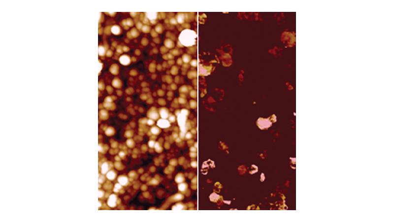
Case Study: Semiconductor Research
PRESENTATION HIGHLIGHTS:
- [00:00:00] Conductive AFM
- [00:06:08] DataCube-SCM on Transistors
- [00:08:06] Conductive AFM Tomography
- [00:09:55] Photo-KPFM on Organic Material
- [00:12:38] Q&A
Case Study: Battery Research
PRESENTATION HIGHLIGHTS:
- [00:00:00] AFM Measurements on Li-Ion Battery
- [00:03:49] Electrical & Mechanical Properties of Cathode
- [00:08:33] Evolution on Graphitic Electrodes
- [00:12:23] Microfabricated Amorphus Silicon Anode
- [00:15:37] Mechanism of Ion & Electron Migration in Composite Solid-State Electrolyte
- [00:19:58] Q&A
Case Study: 2D Materials
PRESENTATION HIGHLIGHTS:
- [00:00:00] Epitaxial Graphene on SiC
- [00:01:21] Suspended Graphene Membranes
- [00:02:51] Programmable Graphene Nanobubbles
- [00:04:08] Graphene: Co-localized Raman & KPFM
- [00:05:20] Moire Pattern on Graphene on hBN
- [00:06:28] Nanoscale Redox Mapping
- [00:08:06] Q&A