Quantitative Characterization of Nanostructured Thin Films
Nanomaterials are usually investigated in the Transmission Electron Microscope (TEM). However, it is possible to characterize nanomaterials quantitatively by benifiting from the large field of view of the Scanning Electron Microscope (SEM). The on-axis TKD technique was developed to this aim; it is now a well established SEM-based method producing orientation distribution measurement at the nanoscale using EBSD hardware. In this application example, the orientation distribution of gold and platinum thin films were measured with e-Flash FS detector retroffited with OPTIMUS TKD head in a FEG-SEM. High speed TKD measurement are achieved at low probe current (<3 nA) allowing to overcome beam drift and achieve ultra high spatial resolution: in 20 minutes over 1000 grains were measured with the smallest grain size being 20 nm and ultrafine features such as twin boundaries were resolved (3nm).


Characterization of Nanostructures with eWARP TKD
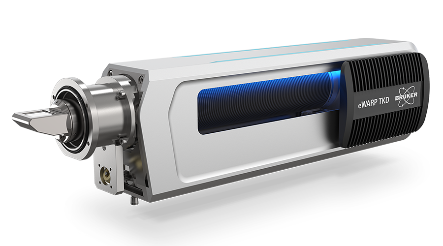
This webnote discusses the characterization of nanostructured thin films using our legacy TKD solution, the eFlash FS detector equipped with an OPTIMUS 2 detector head, which has now been replaced by our next-generation eWARP TKD detector for ultra-fast, high-resolution transmission kikuchi diffraction.
With Bruker's revolutionary eWARP TKD detector, grain structure information can be acquired from thinner layers with improved pattern quality in on-axis geometry, reducing the need for a costly TEM analysis.