Using Nanoelectrical Solutions to Expand the Capability of AFM
Learn About Innovative Nanoelectrical AFM Components & Applications
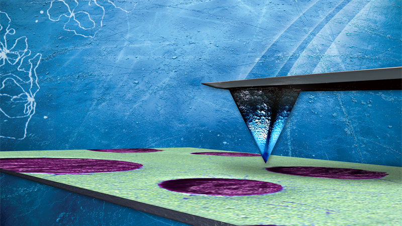
In this webinar, our speaker discusses how AFM-based nanoelectrical measurement capability has advanced. AFM is now more accessible to a wider range of materials and the user can obtain a greater amount of information about their sample than has previously been possible.
Webinar Summary
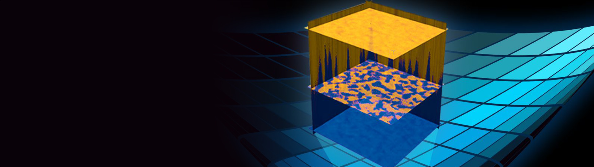
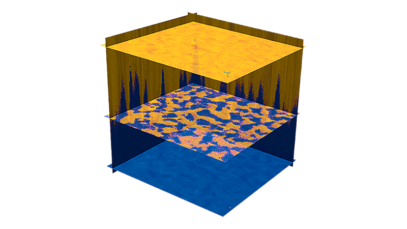
This webinar showcases how correlating nanomechanical and nanoelectrical measurements can lead to a greater determination of properties. The speaker demonstrates how Bruker’s new solution, the NanoElectrical Lab, can correlate both mechanical and electrical data at each single pixel to provide an increased understanding of sample properties while also lengthening the usable lifespan of AFM tips.
During the session, the speakers explore the following topics:
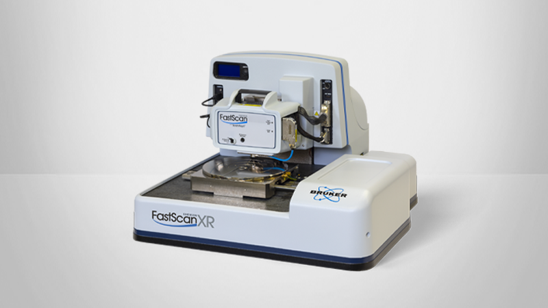
Bruker's NanoElectrical Lab
- Introduction to the NEW DataCube modes
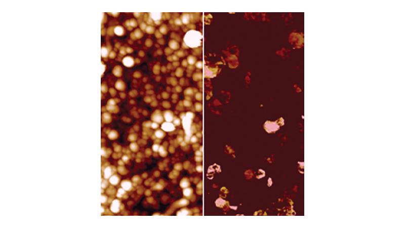
- Correlation of nanomechanical and nanoelectrical data
- Possibilities for tailored nanoelectrical measurements
Nanoelectrical Applications of AFM Instruments
- Graphene and other 2D materials
- Semiconductors
- Nanowires
- Ferro and piezo-electrics
- Smart materials
- Conductive polymers
- Battery materials
- Fuel Cells
This webinar was presented on: March 29, 2018
Find out more more the featured AFM products and services in this webinar:

Speaker

Peter De Wolf, Ph.D., Director of Technology & Application Development
Peter De Wolf is director for AFM technology & application development at Bruker Nano Surfaces, covering all applications related to Scanning Probe Microscopy (SPM). He obtained his PhD from IMEC, Belgium on the development of new SPM methods for 2D carrier profiling in semiconductors and has more than 25 years of experience on SPM. He is the author and co-author of over 30 publications related to electrical characterization using SPM. He also owns several SPM patents, and developed several new SPM modes for electrical characterization.