Displays & Touch Panels
In the popular and growing touch panel and display markets, high accuracy metrology is required to ensure the quality of the end products delivered to the millions of people who purchase and use them. High-quality products with high yield and ultimate reliability are necessary for success in this competitive market space.
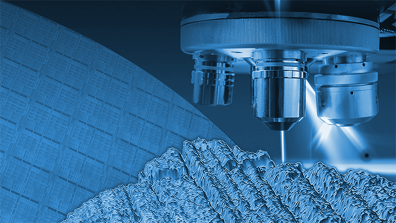
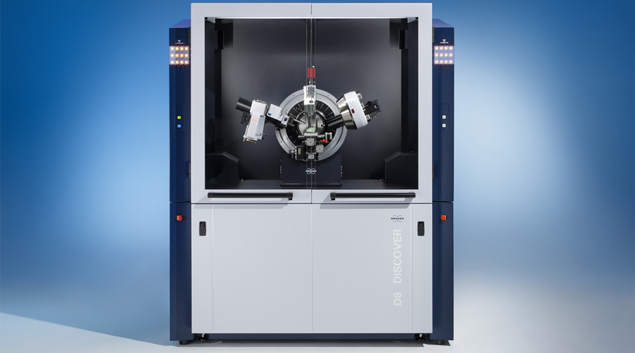
Bruker’s stylus and 3D optical microscope products deliver high-accuracy tactile and non-contact metrology for capacitive ink layer heights, and ITO features, as well as film thickness metrology to the production floor for touch panel and display manufacturing needs.
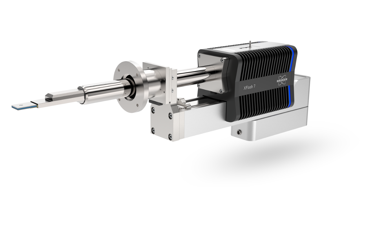
Bruker's electron microscope analyzers, such as EDS for SEM and TEM, EBSD, WDS and Micro-XRF, allow the analysis of texture (EBSD) and the element distributions down to ppm with high spatial resolution and also in layered materials (Micro-XRF). Particularly fast analysis, such as needed in quality control or for large sample areas, is possible using a high collection angle device, such as the Bruker XFlash® FlatQUAD detector.
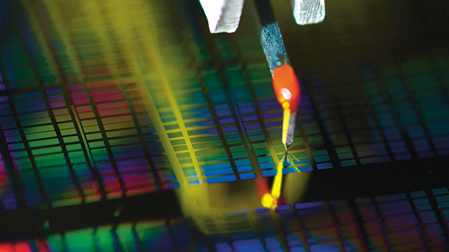
In modern displays, many components and features need to be controlled in order to understand and characterize performance. In addition to the active media, there are fine conductive leads, transparent conductive windows and anti-reflective coatings. Measuring the thickness and composition of such coatings across large surfaces in a non-destructive manner allows for quick and easy failure analysis and development. Micro-XRF is a versatile technique used to investigate many of these features. It can determine the thickness of such leads as well as their composition.
Since yield is king, partner with Bruker for high-quality, high-accuracy metrology that will help improve quality and yield for a wide range of your applications.