Failure and Low-Yield Analysis
Photothermal AFM-IR Spectroscopy Solutions for Failure Analysis
Photothermal AFM-IR spectroscopy combines the high spatial resolution of atomic force microscopy (AFM) with the chemical identification capability of infrared (IR) spectroscopy to allow for the chemical characterization of samples in nanoscale detail
The operating principle for photothermal AFM-IR can be explained in just three simple steps:
- An IR laser pulse arrives on the sample surface under the tip
- The sample absorbs the IR pulse, causing it to heat up and expand, thus applying a mechanical force on the AFM probe
- The magnitude of this force is proportional to the absorption coefficient and can be used to generate an IR spectrum
AFM-IR spectra can be interpreted just like Fourier-transform infrared spectroscopy (FTIR) spectra. Leveraging this ease of nanoscale chemical identification and combining it with the streamlined workflows and ease-of-use of Bruker AFMs provides an ideal solution for analyzing nanocontaminants for failure analysis.
There is a need to discover and eliminate the source of product and device failures to increase throughput, save costs, and increase revenue. Product and device failure in the semiconductor, data storage, polymer, and medical device industries can often be due to surface-level nanocontaminants.
Determining the chemistry of nanocontaminants is essential to identifying their process origin and establishing effective mitigation strategies. Though FTIR is a common method for spectroscopically determining chemistry, it does not provide the nanoscale resolution necessary for characterizing nanocontaminants.
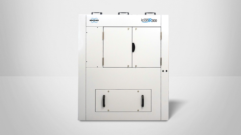
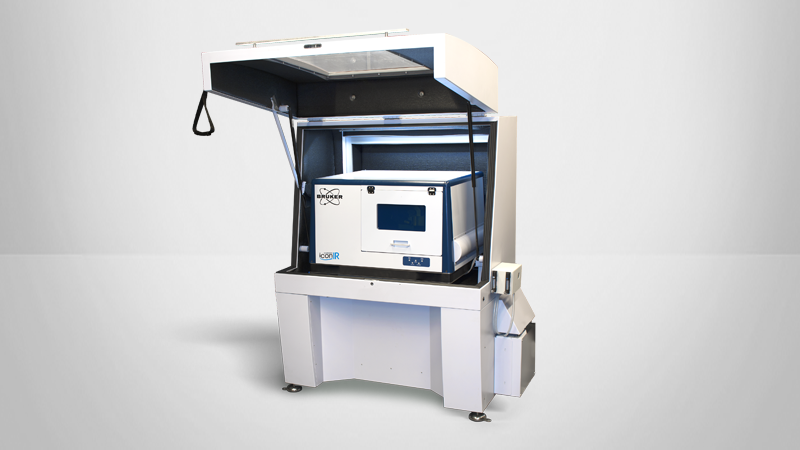
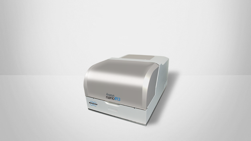
IconIR, IconIR300, and nanoIR3 utilize Bruker's patented photothermal AFM-IR technology to enable high-resolution chemical spectroscopy and imaging. These systems provide unique insight into the chemical nature of nanocontaminants to help understand and mitigate their process origin and drive yield enhancement.
Discover Localized FTIR at the Nanoscale
IR spectroscopic analysis can provide information on the chemistry of nanocontaminants, assisting in process origin identification. FTIR is a standard means of IR spectroscopic analysis, but is limited to a resolution of tens of microns. AFM-IR can achieve a lateral resolution of up to 10 nm and has a close correlation with transmission FTIR spectra in terms of peak shapes, positions, band ratios, and high signal-to-noise ratios. This correlation enables AFM-IR spectra to be interpreted just like FTIR spectra using established spectral libraries like Wiley's KnowItAll.
Access the Power of AFM
With IconIR and IconIR300, the broad capabilities of advanced AFM technology are also accessible. For nanocontaminant detection and identification, it may be valuable to first run a fast survey scan over a large area, searching for locations with a higher topography or a lower modulus. Then, photothermal AFM-IR analysis can be limited to only smaller areas of interest.

Failure analysis and materials characterization groups within industrial companies are focused on solving problems to help improve process development and resolve process-related issues to help their organizations save costs and increase revenue.
The nanoIR3-s provides a complete nanoscale FTIR, chemical imaging, and materials characterization platform. It combines two complementary nanoscale IR techniques, AFM-IR and scattering SNOM coupled with AFM-based materials property mapping. The system is productive and reliable, getting you productive data within a day. Applications include:
Nano-organic contaminants
LowK dielectrics
Semiconductor materials
Data storage media and slide

Organic nano-contaminants are a serious defectivity issue for semiconductor and data storage companies where current characterization techniques have limited capabilities. The nanoIR3 system acquires IR spectra at spatial resolutions down to 10 nm, enabling the measurement of such defects and other semiconductor materials..
The spectra generated using Bruker's patented AFM-IR technique directly correlates with traditional FTIR spectra, and are thus comparable to standard FTIR libraries. In addition to chemical analysis, nanoIR3 provides complementary mechanical, electrical, thermal, and structural property information with nanoscale spatial resolution.