
Electron Microscopes
From Microscopes to Meaningful Analyses
Bruker has a long history with microscope technologies, including electron microscopes. We offer a line of cutting-edge Nion scanning transmission electron microscopes (STEMs), as well as numerous analytical solutions that can be added to the Nion ULTRASTEM or nearly any other electron microscope.
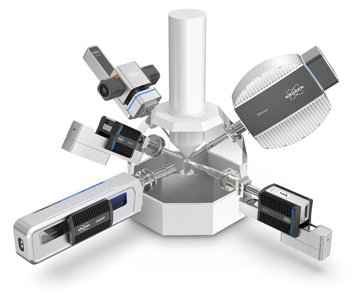
Our Electron Microscope Analyzer range provides a SEM, TEM or STEM with additional analytical capabilities that give users the ability to perform detailed elemental, compositional and microstructural analysis. This range includes industry-leading systems for Energy Dispersive X-ray Spectroscopy (EDS), Wavelength-Dispersive X-ray Spectroscopy (WDS), Electron Backscatter Diffraction (EBSD), and micro-X-ray fluorescence on SEM. We also offer nanomechanical test instruments that are used to assess sample properties during in-situ nanoindentation, compression, or tensile, or bend testing.
Electron Energy Loss Spectroscopy (EELS)
Electron Energy Loss Spectroscopy (EELS) measures the energy loss of the fast-beam electrons that have passed through the sample. For a scanned beam, this generates a spectrum from each point on the sample and can be used to generate an elemental map at atomic resolution using the characteristic loss edges for each element. The electronic structure of the sample can be probed, including the band gap and chemical shifts due to different bonding environments. Nion HERMES also makes it possible to probe the vibrational properties of molecules, and phonons in crystals containing interfaces and defects, at near-atomic resolution.
Ultra-stable Scanning Transmission Electron Microscopes (STEMs)
Bruker's line of Nion scanning transmission electron microscopes light up a world of possibilities in materials research. These cutting-edge instruments enable scientists and engineers to explore sample structures at the atomic scale and probe into atomic interactions in four dimensions. Featuring Python-powered open-source software, our STEMs have been designed from the ground up to enable a new generation of experiments.
Systems include:
Nion ULTRASTEM
With a range of operating voltages between 30 and 200 kV, the Nion ULTRASTEM uses a high-brightness, high-stability cold field emission electron gun (CFEG) that allows higher resolution, higher probe current providing sub-Angstrom resolution imaging, fast nanoanalysis with an atom-sized electron probe, and efficient coupling to a variety of detectors.
Nion HERMES
Bruker’s Nion High Energy Resolution Monochromated EELS STEM, HERMES, combines a high brightness cold field emission gun (CFEG) with a state-of-the-art monochromator and Electron Energy Loss Spectroscopy (EELS) to enable atomic resolution imaging, chemical mapping, 4D-STEM, and vibrational spectroscopy in the electron microscope at the highest level.
Elemental Analysis & Microanalysis on Electron Microscopes
Bruker’s Electron Microscope Analyzers range, including EDS, WDS, EBSD and Micro-XRF on SEM, provides electron microscope users with the tools needed to perform a highly-detailed compositional and structural analysis of their samples. The full integration of these techniques into Bruker’s ESPRIT software means users can easily combine the data obtained by each of these complementary methods.
Nanomechanical Property Analyzers
Bruker’s Hysitron PicoIndenters make it easy to conduct in-situ mechanical experiments in your electron microscope. Our unique transducer design ensures stability throughout the entire experiment, producing precise data even at the nanoscale. Correlating video capture from the microscope with in-situ mechanical testing data enables real-time monitoring to advance nanoscale materials property understanding. Available modes include nanoindentation, compression, tensile, and bend testing, and additional accessories are available to facilitate high- and low-temperature experiments.

