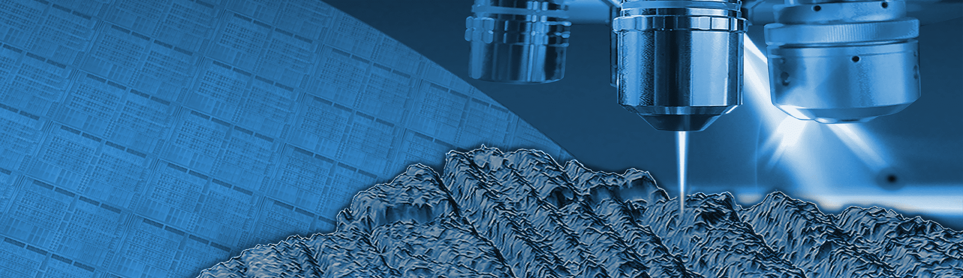
三维光学轮廓仪
快速的非接触式三维轮廓表征
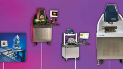
布鲁克是三维表面计量与检测方案的全球领导者,提供快速、可信赖及易用的非接触式三维轮廓表征方案。样品小至显微视场下的MEMS结构,大到完整的机械引擎。这些方案为研发、制造及质量控制的研究者和工程师们提供了业界领先的灵敏度和稳定性。而这正是其它计量方法在精细三维表面测量应用方面所面临的挑战。
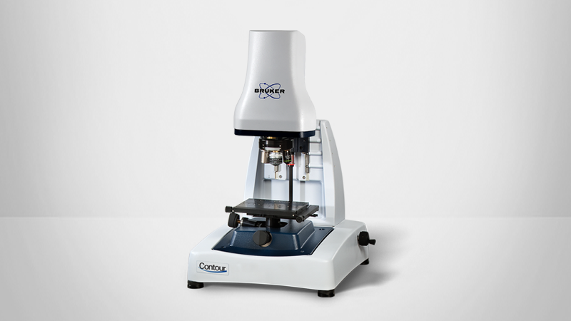
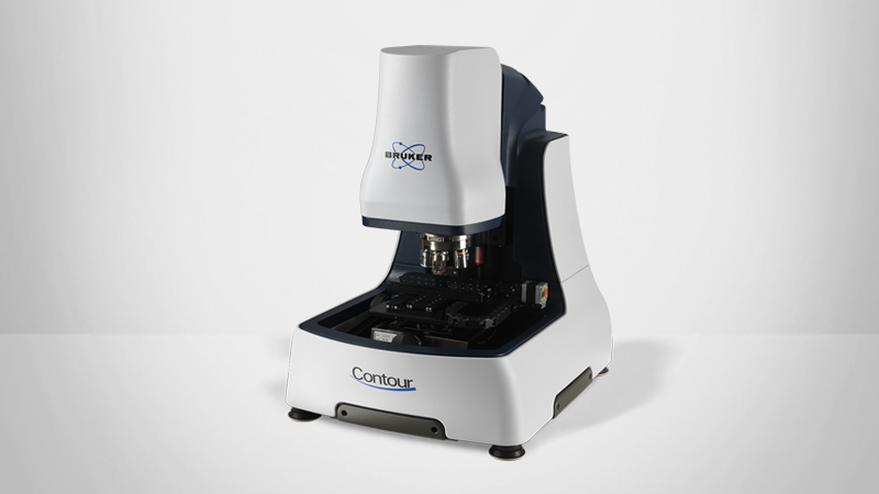
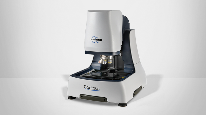
我们的光学轮廓仪基于Wyko®专有核心技术,历经十代积累,提供了其他测量系统无法企及的高精度与稳定性。在今日,这些正成为精密表面三维测量的主流应用场景。我们的计量工具已被证明可支持全球实验室和生产环境中的尖端研究和发现。
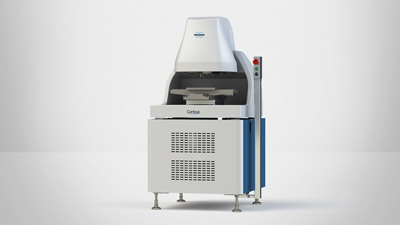
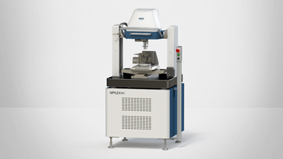
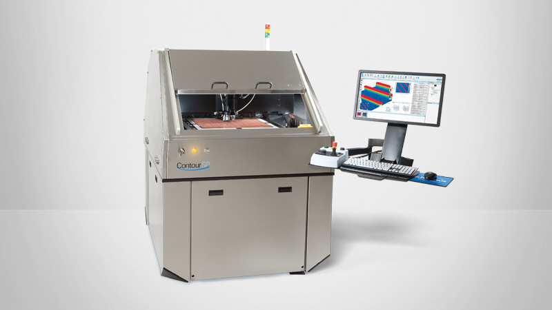
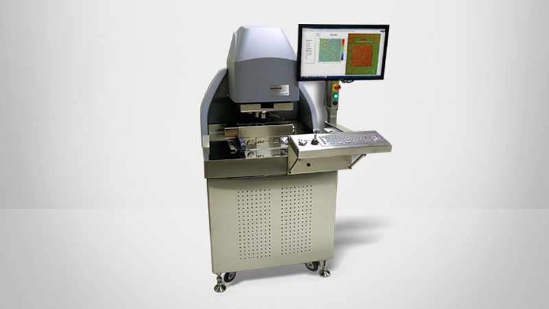
找到最适合您的三维光学轮廓仪
Frequently Asked Questions About 3D Optical Profilers
A 3D optical profilometer is a non-contact, non-destructive metrology system based on optical microscopy that is specifically designed for surface texture and roughness metrology in R&D and manufacturing environments. They collect data areally (over a 2D area) with a single exposure and use that data to generate 3D height maps.
Bruker's 3D optical profilometers utilize coherence scanning interferometry, also known as white light interferometry (WLI), to provide fast, accurate surface measurements over large areas to quantify a variety of surface properties. These profilers are used in engineering, research, and production process control for an extremely wide range of markets, including precision machining, medical, microelectronics, MEMS, semiconductor, solar, data-storage, automotive, aerospace, and material science.
All optical profiling techniques are 3D and quantify the topography of a surface. Optical metrology also includes techniques that are 2D and can be used to measure critical dimensions in the plane of the surface. Common systems used for 2D optical metrology include optical microscopes and scanning electron microscopes. 2D optical metrology is dependent on image contrast and sample optical properties (which may not be directly linked to topography).
Optical profilometry encompasses a wide breadth of non-contact profiling methods. These techniques all use information gained from the reflection of light off the sample surface.
Pattern projection profilometry—A light pattern is projected onto a surface, enabling analysis of the light pattern’s deformation to gain height information. This is often used for form and fit tests of mid-sized parts, such as molds, engine components, and laptops.
3D laser scanning—A laser beam is projected onto an object, and the laser’s time-of-flight before returning is used to determine the object’s position in space. This method is used to document historical objects and perform dimensional inspection of large-scale objects, such as sculptures, buildings, and car doors.
Confocal microscopy—Light is focused through a pinhole optic and 3D data is captured by scanning along the Z axis and reconstructing with only the in-focus portions of each 2D image slice in the stack. Using the pinhole optic prevents out-of-focus light from participating in image formation, limiting the depth of field. Confocal microscopy is a standard imaging technique in many biological science and some materials science applications.
Focus variation—The sharpest points (the most in-focus) from a whole 2D image stack are used to construct the 3D topography of a surface. This method is suitable for a wide range of materials and surfaces.
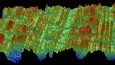
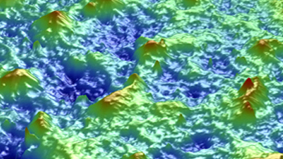
White-light interferometry—Interference patterns are generated using split and recombined light waves. The interference patterns are used to calculate surface topography with nanometer-scale resolution. WLI is used to precisely analyze sub-micron roughness of materials, such as electronics, mirrors, optics, and wafers.
White-light interferometry (WLI), also known as coherence scanning interferometry, is a non-contact optical profilometry method that takes advantage of the nature of light waves to interfere with each other constructively and destructively (i.e., wave superposition). WLI is ideal for applications where speed is critical, parts are large, samples are fragile, or there is non-uniform surface texture. These applications often show up in the research, automotive, semiconductor, biological materials, and additive manufacturing sectors, among many others.
LEARN MORE:
WLI has many advantages inherent to the technique, including:
Magnification-insensitive height resolution—WLI relies on optical interference, which is completely independent of objective lens magnification. This allows for a high vertical resolution alongside a large FOV.
High throughput—As an areal technique, WLI collects many data points at once.
No sample damage—WLI is completely non-destructive, since it is a non-contact profiling method.
Low maintenance—There are no consumables used in WLI, and self-calibrating systems further decrease maintenance requirements.
Deep-trench capabilities—WLI can profile any surface that the objective can “see”, including the bottom of high aspect ratio trenches and even sidewalls when using specialized objectives.
Using a spherical object as an example, a 2D measurement would show a circle, and a 3D measurement would show a full sphere. A 2.5D measurement is between the two, resulting in a hemisphere. Technically, optical profilers extract 2.5D measurements, though it is common to refer to the results as 3D measurements.
There are Bruker WLI systems installed in many different types of facilities, from those that experience ambient conditions to noisy fab environments and cleanrooms. Discuss your facility and requirements with our experts to find the best system for you.


支持

我们能提供哪些支持?
布鲁克致力于为客户解决实际应用问题。我们不断开发新的测试技术,并帮助客户选择最合适的系统与配件。我们通过培训或者延保等方式,与客户保持长久的合作关系。
我们拥有专业的服务团队,支持工程师、应用科学家和专家团队将通过系统服务,功能升级,应用拓展和技术培训等多种方式帮助您最大化的发挥设备的效能。