Hysitron PI 95
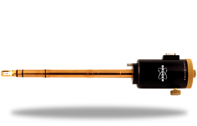
Hysitron PI 95 TEM PicoIndenter
Bruker’s Hysitron PI 95 TEM PicoIndenter is the first full-fledged depth-sensing indenter capable of direct-observation nanomechanical testing inside a transmission electron microscope (TEM). With this side-entry instrument, it is not only possible to image the mechanical response of nanoscale materials, but also to acquire load-displacement data simultaneously. Further, an integrated video interface allows for time synchronization between the load-displacement curve and the corresponding TEM video.
To learn more, continue reading, contact us, or see FAQs about this product.
Customized Solution for Your TEM
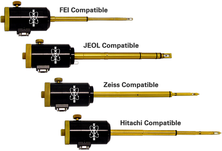
The Hysitron PI 95 has been carefully designed for compatibility with JEOL, FEI, Hitachi, and Zeiss microscopes. With this instrument it is not only possible to image the mechanical response of nanoscale materials, but also acquire quantitative mechanical data simultaneously. The integrated video interface allows for synchronization between the load-displacement curve and the corresponding TEM video.
Optimized for Nanoscale Investigation

The Hysitron PI 95 is uniquely suited for the investigation of nanoscale phenomena. Performing these types of studies in the TEM can provide unambiguous differentiation between the many possible causes of force or displacement transients which may include dislocation bursts, phase transformations, spalling, shear banding or fracture onset.
Unparalleled Performance

The Hysitron PI 95 utilizes three levels of control for tip positioning and mechanical testing. In addition to a three-axis coarse positioner and a 3D piezoelectric actuator for fine positioning, the instrument is equipped with a transducer for electrostatic actuation and capacitive displacement sensing for acquiring quantitative nanoscale mechanical data.
Expand PI 95 TEM's Capabilities
LEARN MORE:
Contact us for more information about available upgrade options and how PI 95 TEM can be configured to meet your specific measurement needs now and grow with your research going forward.
Watch our Recent Broadcasts on Nanomechanics in SEM
Our webinars cover best practices, introduce new products, provide quick solutions to tricky questions, and offer ideas for new applications, modes or techniques.
Frequently Asked Questions
In-situ mechanical testing inside a TEM to measure nanoscale mechanical, electrical, and functional properties of materials with simultaneous high-resolution imaging.
Nanoindentation, compression, tension (with PTP), bending, fatigue, fracture, creep, strain-rate loading, and electromechanical testing (with E-PTP).
1D (nanowires, nanopillars, fibers), 2D (films, membranes, graphene), and 3D microstructures, as well as interfaces (grain boundaries, multilayers, joints).
Direct atomic- to nanoscale observation of deformation, defect nucleation, dislocation motion, fracture, and phase transformations with nanometer resolution.
Typically, the systems can reach up to 1–2 mN load and 1–2 μm of displacement, sufficient for most nanostructures and thin films.
Focused ion beam (FIB) milling or microfabrication methods are commonly used to prepare site-specific TEM lamellae, nanopillars, or suspended structures.
The most common applications include nanomechanics of metals, semiconductors, ceramics, polymers, 2D materials, battery/electrochemical materials, and MEMS/NEMS, as well as thin film reliability and defect dynamics studies.