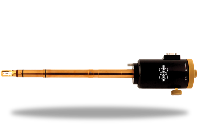
Hysitron PI 95 TEM PicoIndenter
布鲁克的Hysitron PI 95 TEM PicoIndenter 是首台能够直接在透射电子显微镜 (TEM) 内观察的深度感应纳米压痕设备。有了这种测试仪器,不仅能够对纳米级材料的力学响应进行成像,还可以同时获取载荷-位移数据。此外,集成视频接口允许在载荷-位移曲线和对应的 TEM 视频之间进行同步。
To learn more, continue reading, contact us, or see FAQs about this product.
针对您的 TEM 的定制解决方案

Hysitron PI 95 经过精心设计,可与 JEOL、FEI、日立和蔡司显微镜兼容。有了这种仪器,不仅能够对纳米尺度材料的力学反应进行成像,而且可以同时获取定量机械数据。集成的视频接口允许载荷-位移曲线和相应的 TEM 视频同步。
针对纳米级研究进行了优化

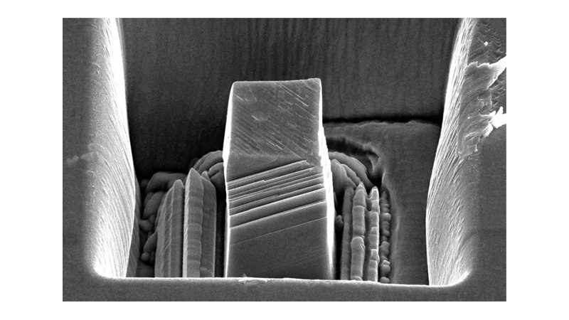
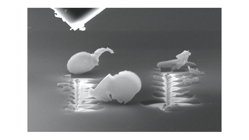
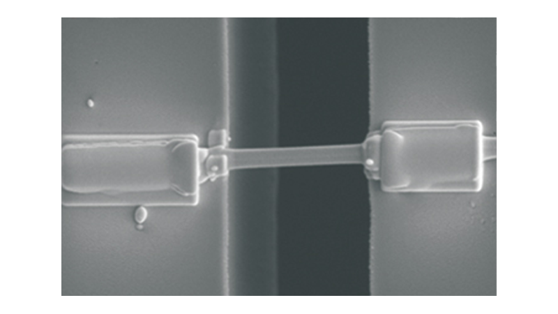
Hysitron PI 95 特别适用于纳米尺度现象的研究。在 TEM 中执行这些类型的研究可以明确区分力或位移瞬变的许多可能原因,这些原因可能包括错位爆发、相变、剥落、剪切带或断裂产生。
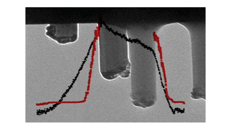
无与伦比的性能

Hysitron PI 95 采用三级控制进行尖端定位和力学测试。除了三轴粗定位器和用于精细定位的三维压电调整器外,该仪器还配备了用于静电驱动的传感器和用于获取定量纳米级力学测试数据的电容位移传感器。

观看电镜内力学性能测试的最新网络研讨会
我们的网络研讨会涵盖最优实践、新产品介绍,提供困难问题的快速解决方案,还包含新应用、新模式与新技术的介绍。
Frequently Asked Questions
In-situ mechanical testing inside a TEM to measure nanoscale mechanical, electrical, and functional properties of materials with simultaneous high-resolution imaging.
Nanoindentation, compression, tension (with PTP), bending, fatigue, fracture, creep, strain-rate loading, and electromechanical testing (with E-PTP).
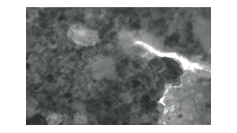
1D (nanowires, nanopillars, fibers), 2D (films, membranes, graphene), and 3D microstructures, as well as interfaces (grain boundaries, multilayers, joints).
Direct atomic- to nanoscale observation of deformation, defect nucleation, dislocation motion, fracture, and phase transformations with nanometer resolution.
Typically, the systems can reach up to 1–2 mN load and 1–2 μm of displacement, sufficient for most nanostructures and thin films.
Focused ion beam (FIB) milling or microfabrication methods are commonly used to prepare site-specific TEM lamellae, nanopillars, or suspended structures.
The most common applications include nanomechanics of metals, semiconductors, ceramics, polymers, 2D materials, battery/electrochemical materials, and MEMS/NEMS, as well as thin film reliability and defect dynamics studies.