ハイジトロンPI 95

ハイジトロン PI 95 TEM ピコインテンター
ブルカーのHysitron PI 95 TEM PicoIndenter(ハイジトロン PI 95 TEM ピコインデンター)は、透過型電子顕微鏡(TEM)内でナノ力学試験を直接観察できる装置です。現在および将来の幅広い材料研究のニーズにお応えできるように、PI 95には加熱測定、電気特性評価、トライボロジー(スクラッチ)測定など、様々なアップグレードオプションを取り付けることができます。
To learn more, continue reading, contact us, or see FAQs about this product.
TEM 向けのカスタマイズされたソリューション

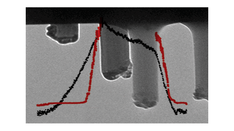
PI 95はFEI、日立、日本電子、Zeiss製の多くのTEMに適応できるようにインターフェイスが設計されています。そのため、TEMにてナノスケールの材料の力学応答を画像化しながら、同時に定量的な力学測定データを取得することができます。ビデオインターフェースを用いることで、荷重-変位曲線のデータとTEMビデオのデータを同期することが可能です。
ナノスケールの材料特性を直性見る

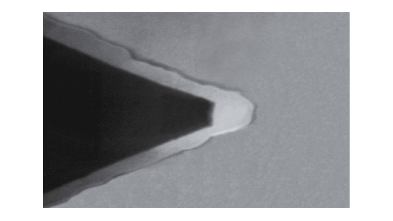
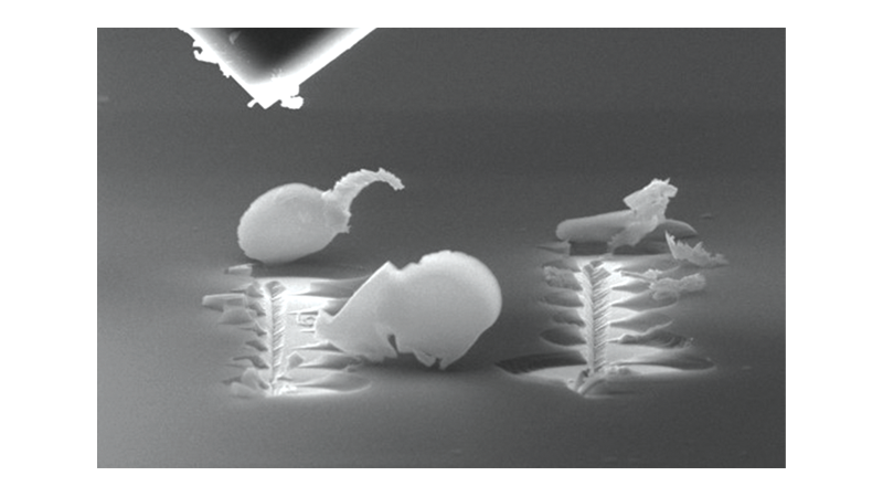
PI 95はナノスケールの力学現象の調査に極めて適しているツールです。転位バースト、相変態、はく離、せん断帯形成、破壊開始など力学試験において荷重または変位の変化が生じる事象は様々ありますが、TEM中でナノ力学試験を実施することにより、これらを明白に区別・把握できます。
高いパフォーマンスを実現

ハイジトロンPI95は、圧子・測定箇所の位置決めのために、3軸粗動ポジショナーと精密位置決め用の3D圧電アクチュエーターを採用しています。また、正確な力学試験のために、静電容量型トランスデューサーと定量的な測定データを取得する静電アクチュエーターを搭載しています。
Watch our Recent Broadcasts on Nanomechanics in SEM
Our webinars cover best practices, introduce new products, provide quick solutions to tricky questions, and offer ideas for new applications, modes or techniques.
Frequently Asked Questions
In-situ mechanical testing inside a TEM to measure nanoscale mechanical, electrical, and functional properties of materials with simultaneous high-resolution imaging.
Nanoindentation, compression, tension (with PTP), bending, fatigue, fracture, creep, strain-rate loading, and electromechanical testing (with E-PTP).
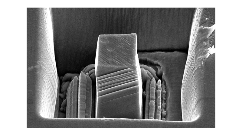
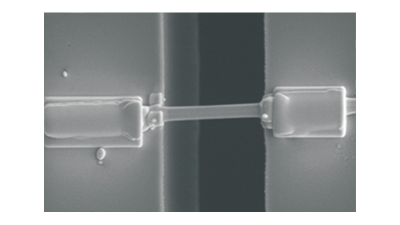
1D (nanowires, nanopillars, fibers), 2D (films, membranes, graphene), and 3D microstructures, as well as interfaces (grain boundaries, multilayers, joints).
Direct atomic- to nanoscale observation of deformation, defect nucleation, dislocation motion, fracture, and phase transformations with nanometer resolution.
Typically, the systems can reach up to 1–2 mN load and 1–2 μm of displacement, sufficient for most nanostructures and thin films.
Focused ion beam (FIB) milling or microfabrication methods are commonly used to prepare site-specific TEM lamellae, nanopillars, or suspended structures.
The most common applications include nanomechanics of metals, semiconductors, ceramics, polymers, 2D materials, battery/electrochemical materials, and MEMS/NEMS, as well as thin film reliability and defect dynamics studies.