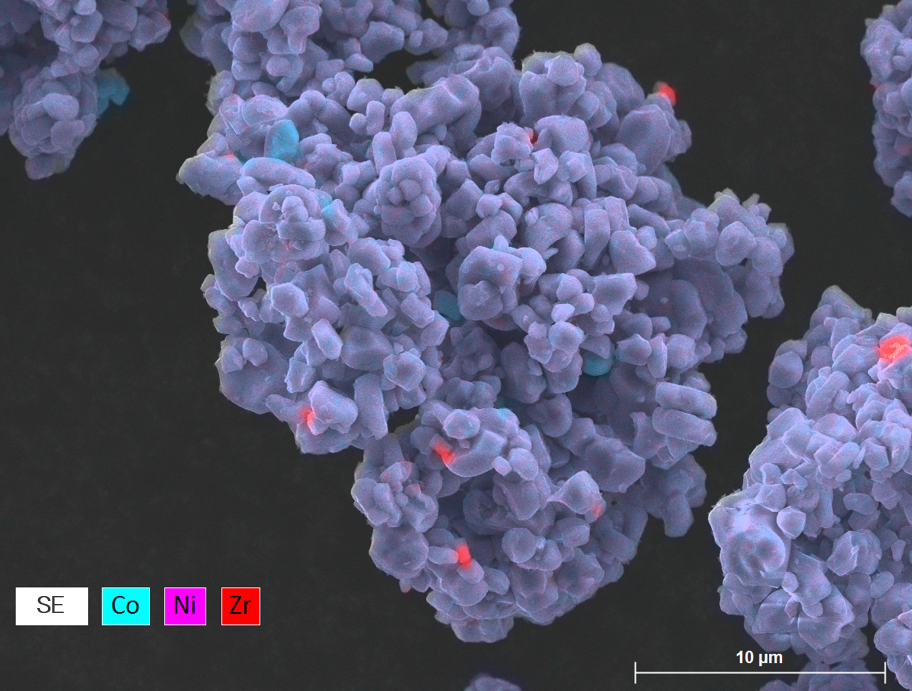
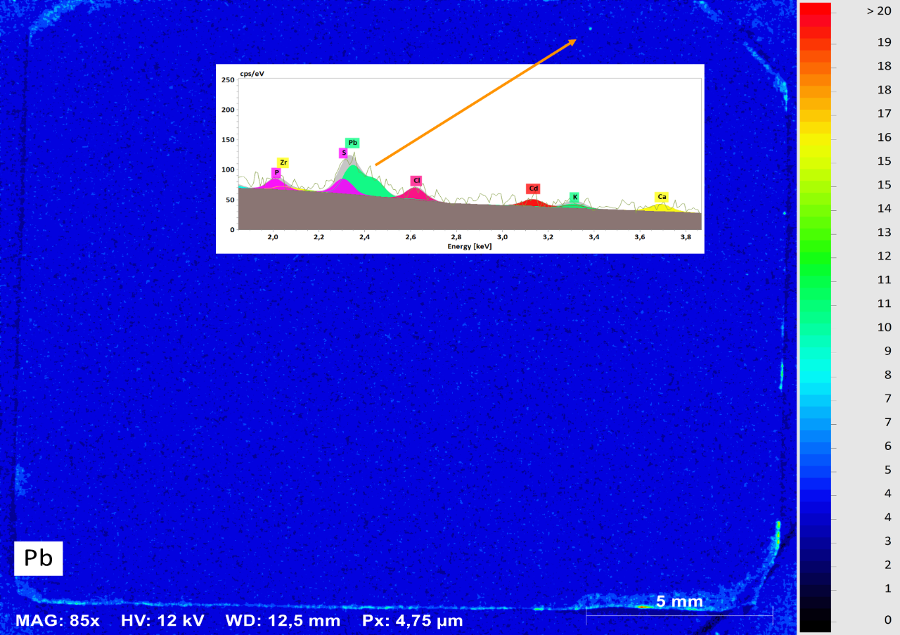
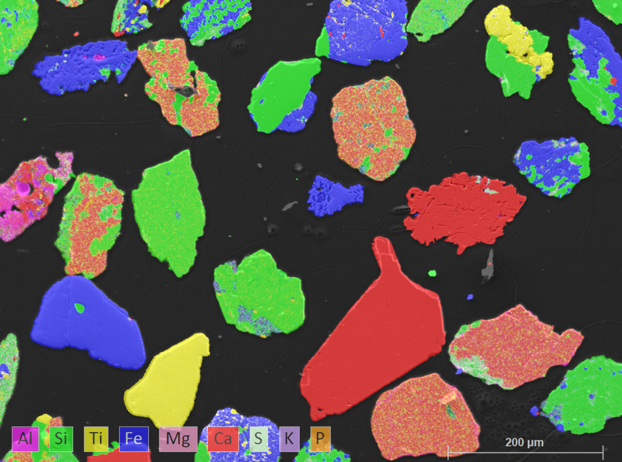
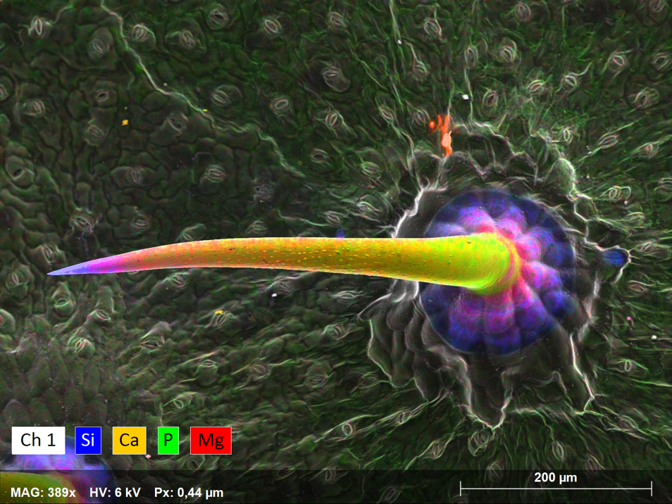
电子显微镜分析仪

QUANTAX FlatQUAD

更高的X射线探测效率

优越的处理能力  

为电子束敏感的样品量身打造

Overcome the Limitations of Conventional EDS with QUANTAX FlatQUAD

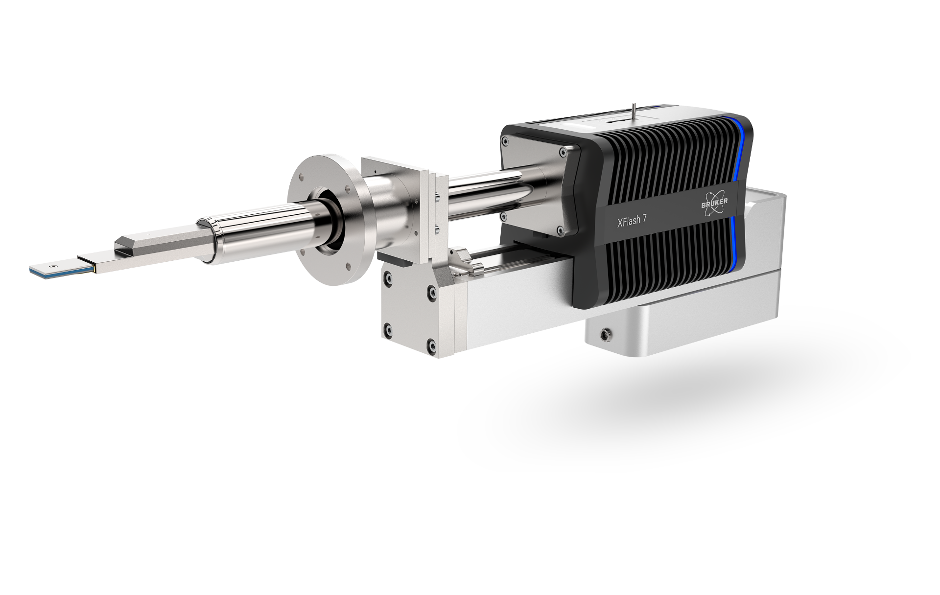
QUANTAX FlatQUAD is the advanced EDS microanalysis system that uses the revolutionary XFlash FlatQUAD 2L detector, whose unique design maximizes collection efficiency for unrivalled mapping performance, even with challenging samples.

QUANTAX FlatQUAD contains everything you need to perform advanced Energy Dispersive X-ray Spectroscopy (EDS), including detector, electronics and Bruker's comprehensive ESPRIT software platform

A Unique Geometry to Expand the Possibilities of EDS

EDS Analysis at Industry-Leading Throughputs  

  • Ultra-efficient X-ray collection: industry-leading solid angle of >1.1 sr
  • Extremely fast analysis at output count rate of 4,000,000 cps. 
  • More than 10 times faster than other available large-area detectors.  


Ultra-High Resolution Mapping 

  • High collection efficiency for nanoscale elemental mapping.
  • Annular detector design enables parallel SE / BSE imaging.
  • Quantitative and qualitative analysis from one detector. 


Elemental Analysis of Challenging Samples 

  • Analyse sensitive and insulating samples at low kV or in low vacuum mode.
  • High take-off angle for minimal shadowing effects for samples with high topography. 


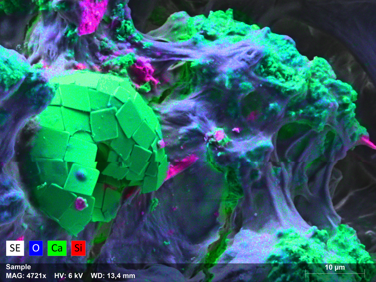
The unique geometry of QUANTAX FlatQUAD's detector maximizes the collection of the EDS signal (magenta) whilst enabling detection of the BSE signal (blue).  


Learn more about how QUANTAX FlatQUAD is enabling advanced EDS analysis in this customer testimonial.

Taking Energy Dispersive Spectroscopy to the Next Level

The unique design of the XFlash FlatQUAD 2L EDS detector used in QUANTAX FlatQUAD enables performance beyond the limits of conventional SEM EDS systems. 

QUANTAX FlatQUAD gives users the ability to quickly and easily analyze a wide range of samples that are challenging for conventional systems. 

New feature

Simultaneous Correlated EDS and BSE Imaging

The aperture of the XFlash® FlatQUAD 2L detector is large enough to accommodate the unobstructed transmission of backscattered electrons to BSE detectors on electron microscopes enabling the direct correlation of elemental composition (EDS) and compositional contrast (BSE) from exactly the same beam interaction volume.

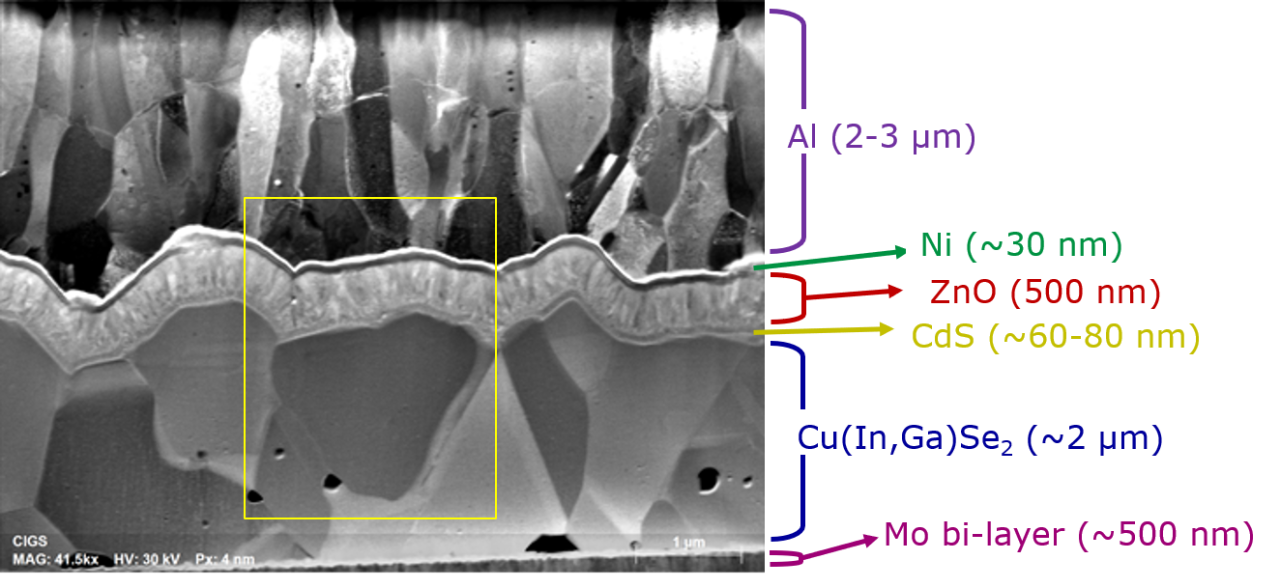
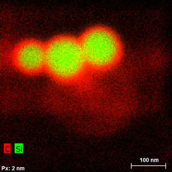
Simultaneous EDS and BSE imaging accelerates materials characterization and delivers perfectly registered multimodal datasets, all while keeping the electron dose on sensitive samples minimal. This combined approach is especially beneficial for applications that require rapid analysis of elemental distributions, interfaces, contamination, coatings, defects, and degradation processes, such as semiconductors and FIB lamellae, battery materials, nanoparticles and life science samples.

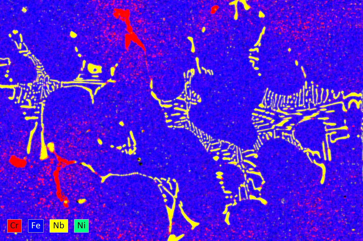
The nanoscale niobium precipitates that strengthen modern engineering steels become clearly visible in this FlatQUAD EDS map. Acquired at 15 kV and 400 pA in only 20 minutes, the map reaches 298 kcps and resolves features approximately 120 nm in size, supporting rapid characterization of performance-critical steel microstructures.

电子束敏感样品的能谱面分布

有些样品,比如生物样品和半导体样品,对于传统能谱来说经常是无法检测的,而XFlash® FlatQUAD 则可以轻松突破这种限制。

与传统的EDS不同,XFlash® FlatQUAD 的高采集效率使之可以在更低的电压和束流下没有信号的损失,这正是避免电子束敏感样品在能谱分析中所必须的条件,此外,使用FlatQUAD进行能谱面分布检测也可以大大减少样品制备过程,经常不需要进行样品的制备。

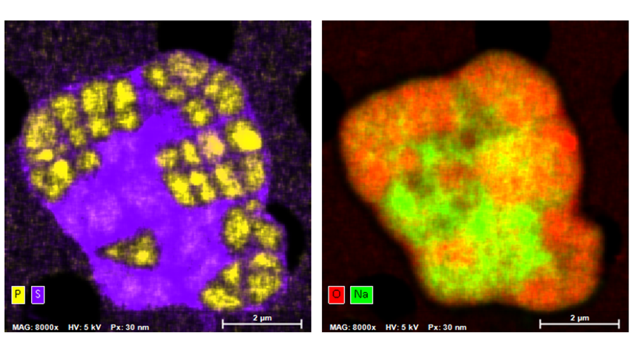
厚度为100nm树脂横截面癌细胞的元素分布图,测试条件 5 kV, 580 pA, 109,800 cps

高计数率下的超快能谱面分布


 XFlash® FlatQUAD探头的独特设计具有高达 3,200,000 cps 的处理能力,配合优良的探头立体角和环形的采集角度,使得用户可以在几秒内完成以往传统EDS需要几个小时的工作。同时,更高的采集效率使得电子束敏感样品所必须的低电压小束流的检测也可以很快完成。


元素成分分布图:15 kV, 3 nA电流下,几秒钟得到的单帧面分布图,计数率 1,169,000 cps,共2800万光子。

高空间分辨率EDS/SEM面分布

得益于XFlash® FlatQUAD探头优越的立体角和采集效率,QUANTAX FlatQUAD实现了超高空间分辨率。

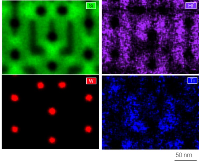
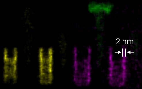
在能谱分析中,要得到很高的空间分辨率,需要使用更低的加速电压和电子束流,这对传统的EDS来说是很大的挑战,而XFlash® FlatQUAD优良的设计和高达1.1 Sr 的立体角使之可以在低至pA级的束流下还能保持很高的灵敏度。这使得QUANTAX FlatQUAD成为低荧光产额样品检测的理想工具,例如:FIB制备的薄片样品和铜网上的纳米颗粒样品。

FinFET 元件的高分辨SEM EDS面分布,5 kV, 1.1 nA, 309,000 cps

不平整的立体样品能谱面分布

QUANTAX FlatQUAD可以有效减少不平整样品的阴影效应。

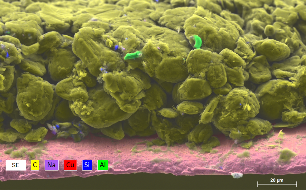
QUANTAX FlatQUAD采用了环形的XFlash® FlatQUAD探头,显著提高了探头的检测角,再结合其大立体角和灵敏度,使用户可以对样品的各个位置特征进行面分布分析,而不是以往只能对一部分能检测到的区域进行分析。

例如在电池工业中,可以用于观察电极材料在充/放电过程中元素分布的变化情况。

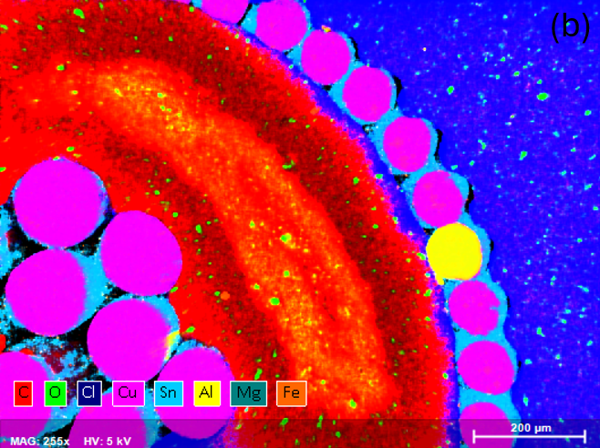
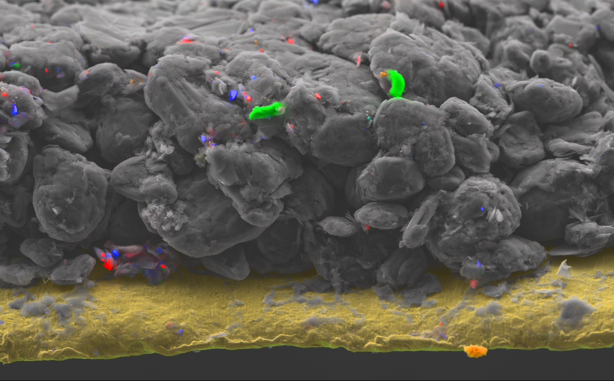
使用BRUKER XFlash® FlatQUAD得到的石墨电极极片样品的截面元素面分布

不导电样品的元素面分布

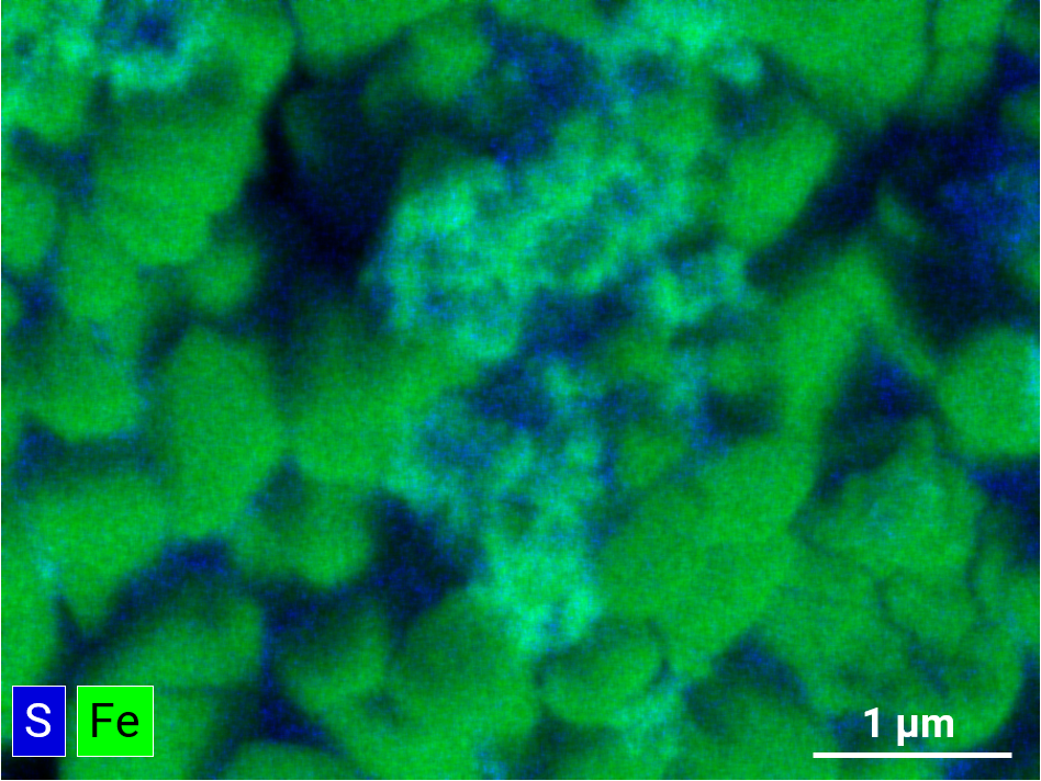
XFlash® FlatQUAD探头的大立体角和高灵敏度使之可以在pA级束流下对样品进行分析,因此可以实现对传统EDS来说很难的样品进行分析,比如:

  • 不导电样品可以在高真空不镀碳的情况下进行分析,这样会减少积碳污染和电子裙散的干扰。
  • 分析碳含量较低的样品,使得由于积碳污染引起的碳含量过高的问题可以得到很好的抑制。
  • 针对贵重样品(如古董等)进行无损检测。


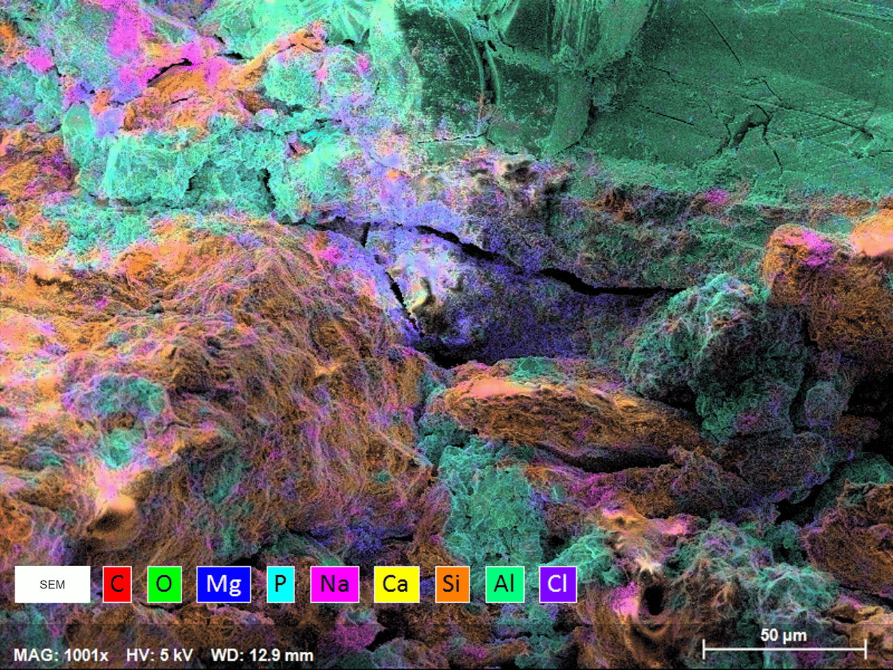
在超低电流< 18 pA 3,100 cps条件下得到的重度充电药片的SEM图像和元素分布图

STEM in SEM Imaging of Electron Transparent Samples

QUANTAX FlatQUAD gives users the ability to perform STEM in SEM EDS measurements of electron transparent samples using just a SEM. This allows for high-resolution EDS without the stringent sample preparation and conditions required for a TEM.

Combined EDS with EBSD on Electron Transparent Samples

To gain even more information from your electron transparent samples, combine QUANTAX EBSD with an eWARP TKD detector.

Chemical distribution map of a 50 nm thin FIB/STEM lamella from AlGaN LED semiconductor device acquired at 5 kV, 960 pA, with 218,400 cps OCR.

样品元素成分的定量分析

 XFlash® FlatQUAD可以对样品的元素成分进行准确的定量分析。

QUANTAX FlatQUAD甚至可以对轻元素例如硼元素进行定量,且最大输出计数率可达3,200,000 cps。

嵌入黄铜块中的BN样品的定量分析

3kV条件下显示硼(B)与氮(N)的比例为符合预期的1:1

使用ESPRIT™ LiveMap进行实时面分布分析

使用XFlash®  FlatQUAD探头可以在ESPRIT LiveMap软件的控制下对样品进行高计数率的实时元素面分布分析。

这对于样品的实时观测是十分有用的,尤其是对样品中某个感兴趣的区域进行实时观测时-例如污染、界面、痕量元素定位- 在实时观测之后可以直接用同一个探头进行进一步的定量分析。 ESPRIT LiveMap功能包含自动元素识别功能和分峰功能。

视频展示了使用ESPRIT LiveMap实时元素映射Sn-Cu焊料区域的过程

One EDS Detector for Every Task - Perform Both Qualitative & Quantitative Analysis

In addition to the unique analytical capabilities of QUANTAX FlatQUAD, which brings EDS to new application fields, it's core XFlash® FlatQUAD 2L detector also works as a standard EDS detector. 

This means that both the qualitative and quantitative EDS analysis of samples is possible using just one EDS detector.  

Discover Applications for QUANTAX FlatQUAD 

The unique geometry of QUANTAX FlatQUAD's detector makes challenging EDS easy, opening up whole new application areas to EDS analysis. 

View other QUANTAX FlatQUAD applications:

Launch webinar

Register Now: Step Into The Future of SEM Elemental Analysis

In this launch webinar, discover XFlash® FlatQUAD™ 2L, the first EDS detector to uniquely combine industry-leading X-ray collection efficiency with the ability to perform parallel BSE imaging.

See how co-registered elemental and contrast information can be acquired simultaneously at lower electron doses enabling faster workflows and higher spatial resolutions, even with beam-sensitive samples.


View More EDS Webinars

Ultra-high resolution elemental map of a nanoscale feature on a semiconductor
ON DEMAND SESSION - 54 MINUTES

Ultra-High Spatial Resolution EDS Mapping of Semiconductors using FEG-SEM

In this webinar we demonstrate the strengths of SEM EDS for the chemical mapping of complex structures in bulk and of electron transparent specimens at a high spatial resolution. Sample analysis using a TESCAN Xe Plasma FIB-SEM and a TESCAN Ga FIB-SEM will be explored.
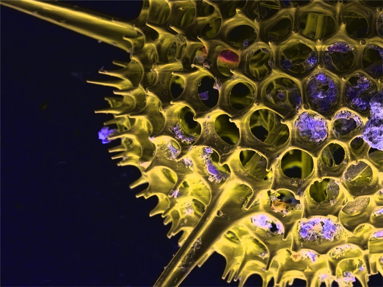
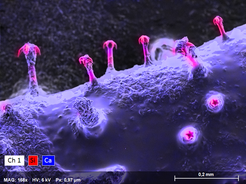
elemental map showing the silicon-based exoskeleton of a Radiolaria/Radiozoa
ON-DEMAND SESSION - 41 MINUTES

Transform Challenging EDS Measurements into Routine Analytical Work

Learn how the Bruker XFlash® FlatQUAD detector can transform your SEM EDS elemental analysis from a slow, difficult, and sometimes impossible - to an easy routine analysis.
eds-sem-biological-sample
ON DEMAND SESSION - 49 MINUTES

Elemental Analysis of Microbiological Samples using SEM EDS

In this webinar we demonstrate how the latest EDS detector technology can be used for the elemental mapping of biological samples. 
arrows
ON DEMAND SESSION - 57 MINUTES

Elemental Mapping (EDS) for the Optimization of Battery Materials and Processes

In this webinar, we focus on energy dispersive X-ray spectroscopy (EDS) coupled with other characterization techniques to see how their usage can offer critical insights regarding battery cell performance and failure diagnostics.
elements-battery-electrode-topographic-eds-sem
ON DEMAND SESSION - 29 MINUTES

Overcome the Limitations of Conventional EDS with QUANTAX FlatQUAD

The new Bruker QUANTAX FlatQUAD system revolutionizes SEM EDS elemental analysis, making it routine and easy - Discover how in this webinar! 
cryo-sem-eds-silk-worm-elemental-map
ON DEMAND SESSION - 40 MINUTES

Analytical Cryo-SEM EDS Mapping for Biological and Life Science Applications

The XFlash® FlatQUAD detector enables the study of beam-sensitive organic materials, particularly frozen biological samples in scanning electron microscopy (SEM). In this webinar we explore the workflow for cryo-SEM-EDS with an example of research on silk worms.