
QUANTAX FlatQUAD
Unmatched Throughput
Analyzing Sensitive Samples
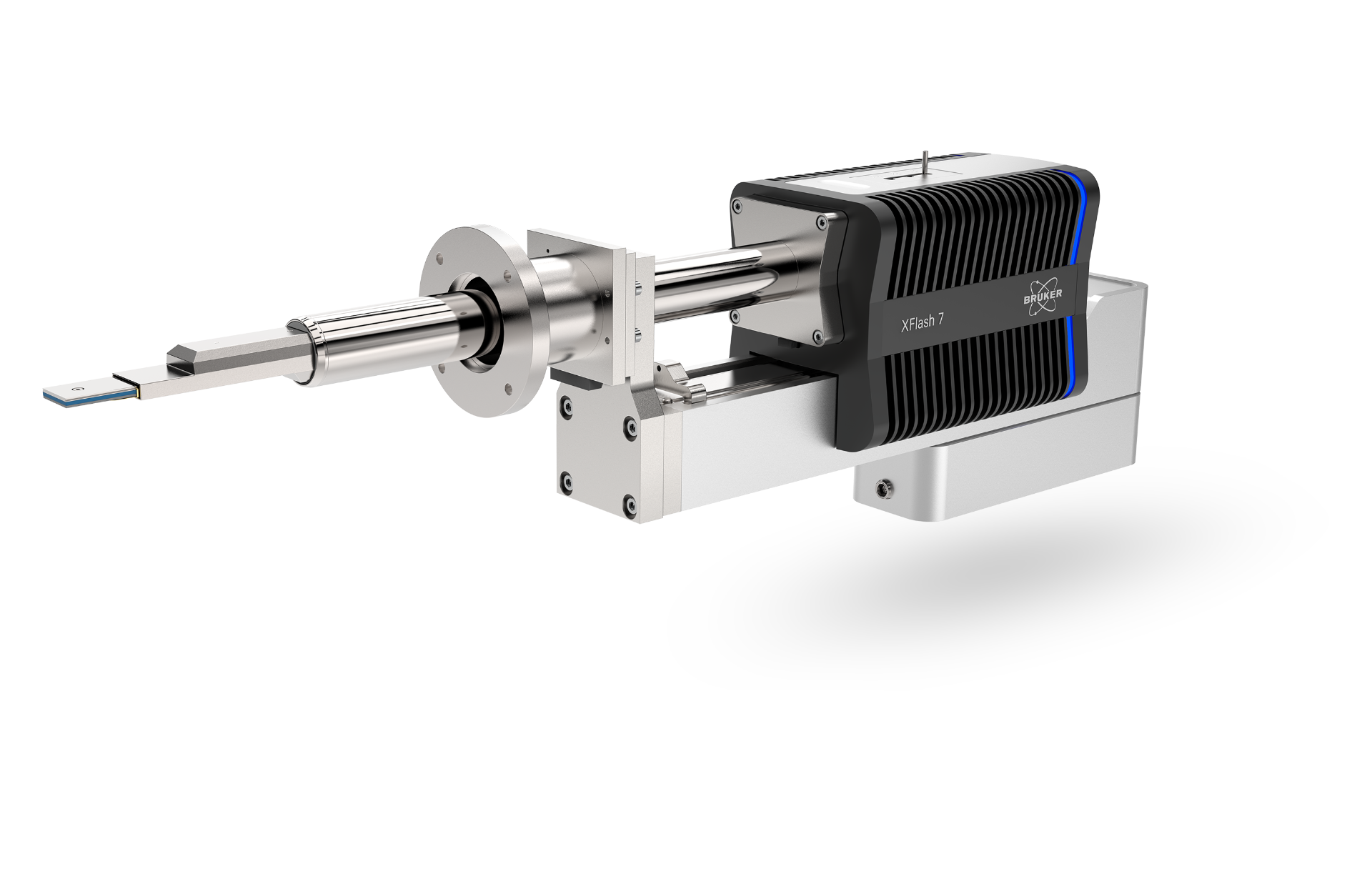
Overcome the Limitations of Conventional EDS with QUANTAX FlatQUAD
QUANTAX FlatQUAD is the advanced EDS microanalysis system that uses the revolutionary XFlash FlatQUAD 2L detector, whose unique design maximizes collection efficiency for unrivalled mapping performance, even with challenging samples.
QUANTAX FlatQUAD contains everything you need to perform advanced Energy Dispersive X-ray Spectroscopy (EDS), including detector, electronics and Bruker's comprehensive ESPRIT software platform.
A Unique Geometry to Expand the Possibilities of EDS
EDS Analysis at Industry-Leading Throughputs
- Ultra-efficient X-ray collection: industry-leading solid angle of >1.1 sr.
- Extremely fast analysis at output count rate of 4,000,000 cps.
- More than 10 times faster than other available large-area detectors.
Ultra-High Resolution Mapping
- High collection efficiency for nanoscale elemental mapping.
- Annular detector design enables parallel SE / BSE imaging.
- Quantitative and qualitative analysis from one detector.
Elemental Analysis of Challenging Samples
- Analyse sensitive and insulating samples at low kV or in low vacuum mode.
- High take-off angle for minimal shadowing effects for samples with high topography.

Taking Energy Dispersive Spectroscopy to the Next Level
The unique design of the XFlash FlatQUAD 2L EDS detector used in QUANTAX FlatQUAD enables performance beyond the limits of conventional SEM EDS systems.
QUANTAX FlatQUAD gives users the ability to quickly and easily analyze a wide range of samples that are challenging for conventional systems.
Simultaneous Correlated EDS and BSE Imaging
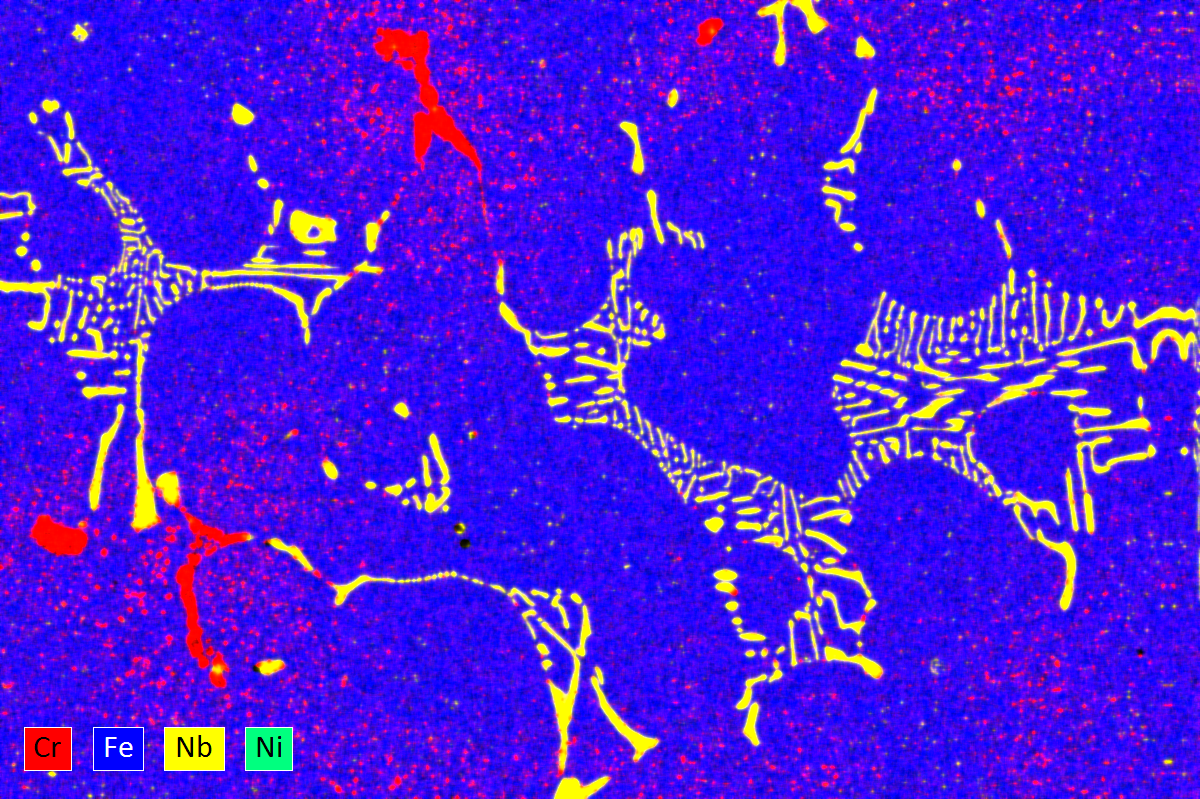
The aperture of the XFlash® FlatQUAD 2L detector is large enough to accommodate the unobstructed transmission of backscattered electrons to BSE detectors on electron microscopes enabling the direct correlation of elemental composition (EDS) and compositional contrast (BSE) from exactly the same beam interaction volume.
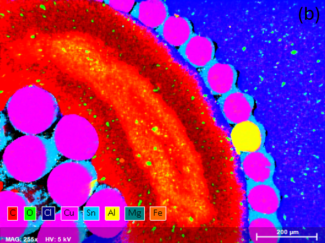
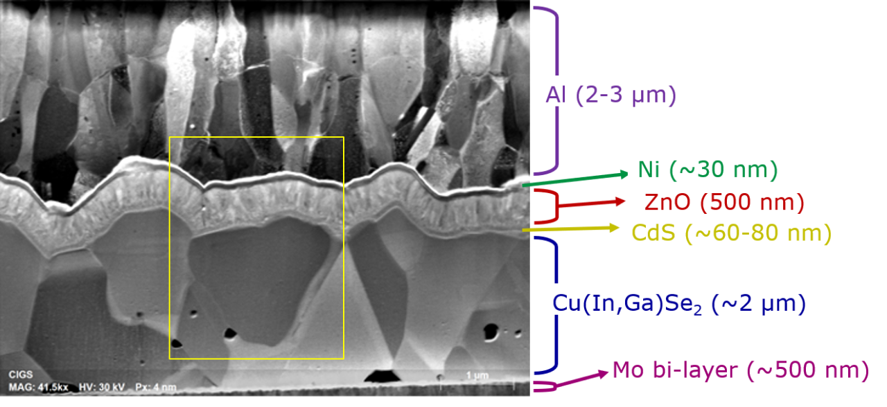
Simultaneous EDS and BSE imaging accelerates materials characterization and delivers perfectly registered multimodal datasets, all while keeping the electron dose on sensitive samples minimal. This combined approach is especially beneficial for applications that require rapid analysis of elemental distributions, interfaces, contamination, coatings, defects, and degradation processes, such as semiconductors and FIB lamellae, battery materials, nanoparticles and life science samples.


Elemental Mapping of Beam Sensitive Samples
The elemental mapping of delicate samples, such as biological and semiconductor specimens, is often impossible. The XFlash® FlatQUAD detector overcomes this limitation with ease.
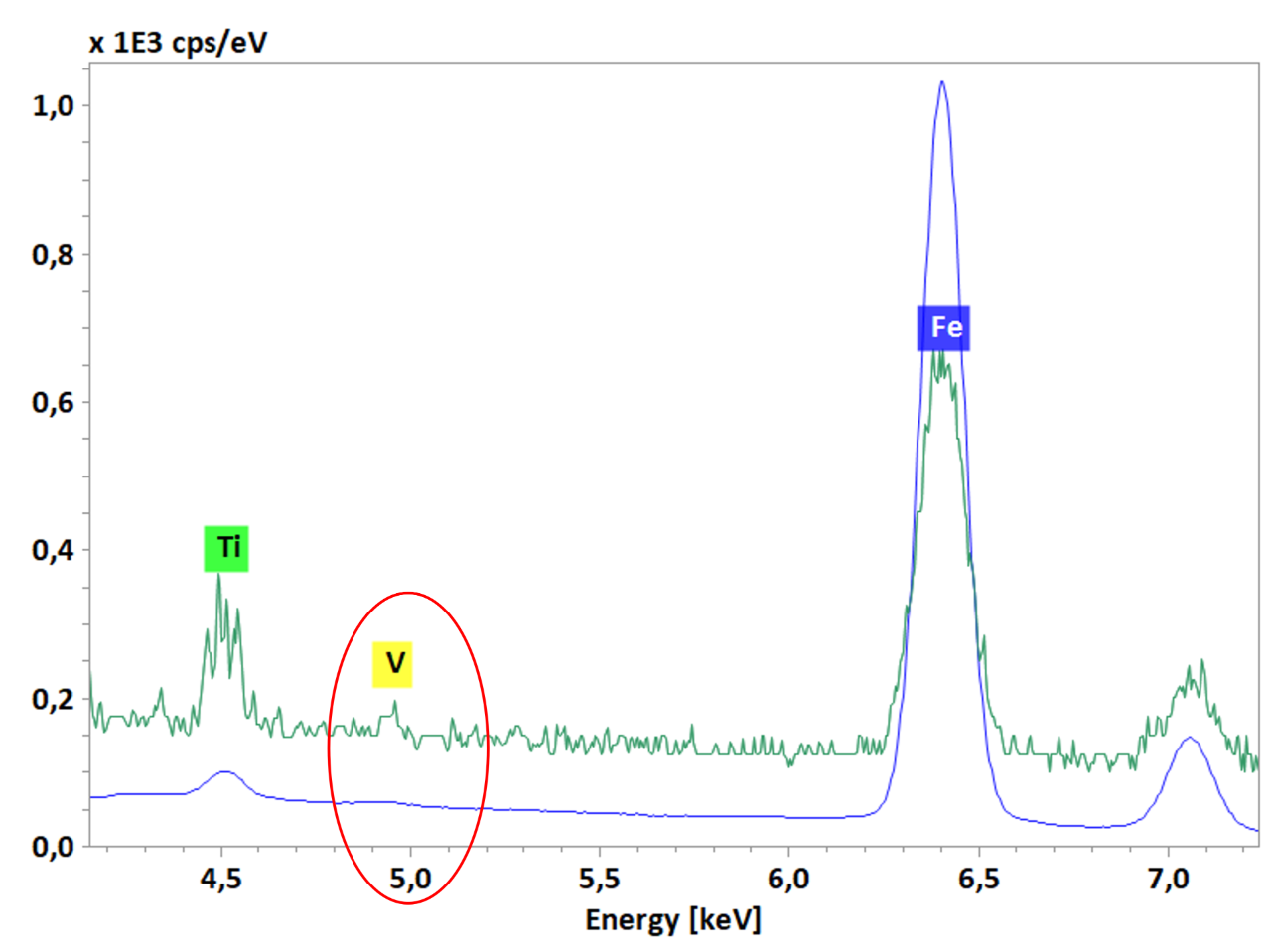
The high collection efficiency of XFlash® FlatQUAD means that elemental mapping can be carried out at low beam current and voltage conditions without the loss in quality seen using a conventional EDS detector. Such conditions are needed to prevent sample damage during hyperspectral imaging. In addition, elemental mapping using FlatQUAD minimizes the need for sample preparation, with often no sample preparation required.

Ultra-Fast EDS Analysis at an Unmatched Throughput
Thanks to its novel design the XFlash® FlatQUAD detector can reach industry-leading output count rates (OCR) of up to 3,200,000 cps – providing the fastest EDS measurements possible using a single EDS detector. This unmatched analysis speed is the result of the detector’s optimized geometry and annular design, which provides a maximized solid angle, alongside ultra-fast parallel signal processing.
Using QUANTAX FlatQUAD users can make elemental measurements within seconds that would take hours using a conventional detector, allowing researchers to work through more samples in less time. The high collection efficiency of the XFlash® FlatQUAD detector means that fast elemental mapping can take place even at low electron doses, i.e. the low probe currents and acceleration voltages required for the analysis of beam-sensitive samples.

Ultra-High Resolution EDS in a SEM
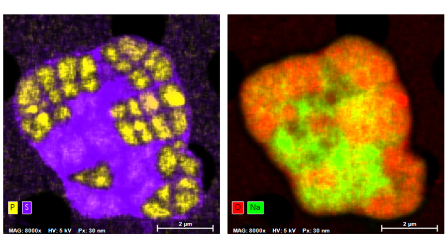
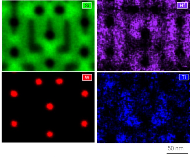
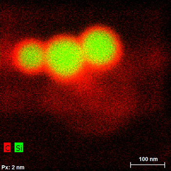
Ultra-high spatial resolution elemental mapping is possible using QUANTAX FlatQUAD thanks to the high solid angle and collection efficiency of the XFlash® FlatQUAD detector.
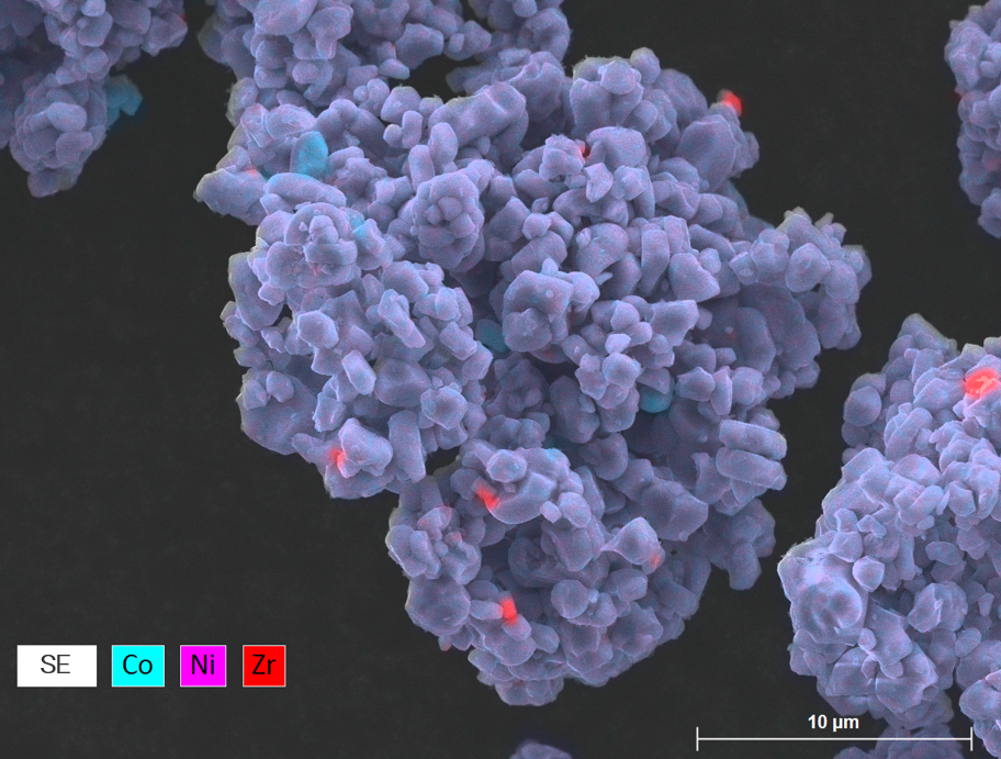
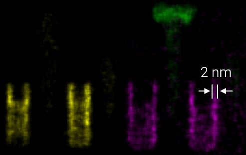
In order to resolve fine features the acceleration voltage and probe current must be kept in an appropriate range. These conditions are very challenging for conventional EDS systems however XFlash® FlatQUAD's optimized geometry and large solid angle (1.1 sr) mean it is highly sensitive, allowing for precise analysis in the low pA range.
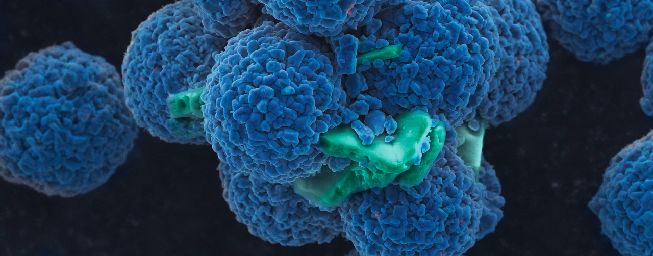
This sensitivity makes QUANTAX FlatQUAD ideal for the mapping and analysis of low X-ray yield samples such as FIB lamella and nanoparticles on a grid.

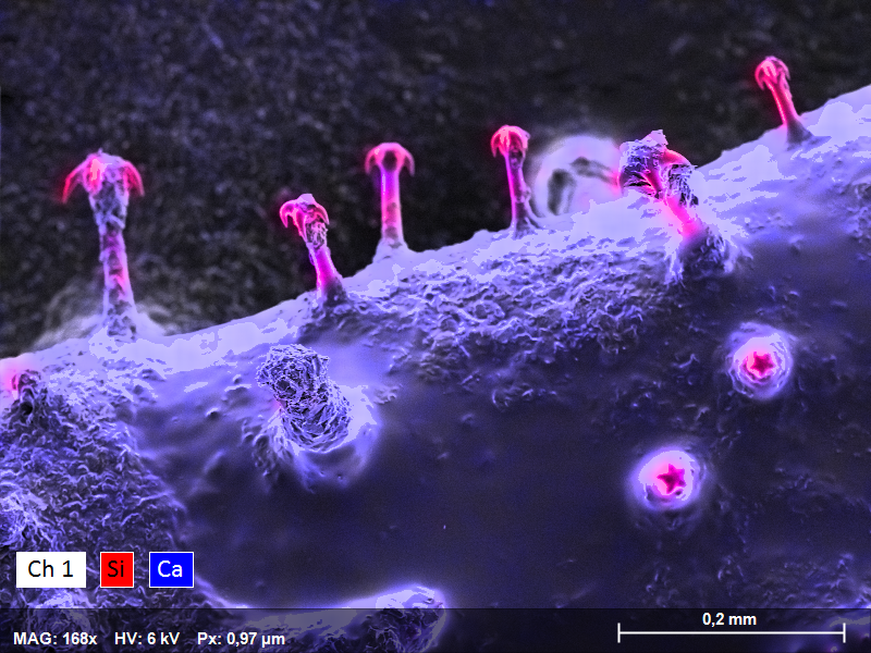
Elemental Mapping of Topographic Samples
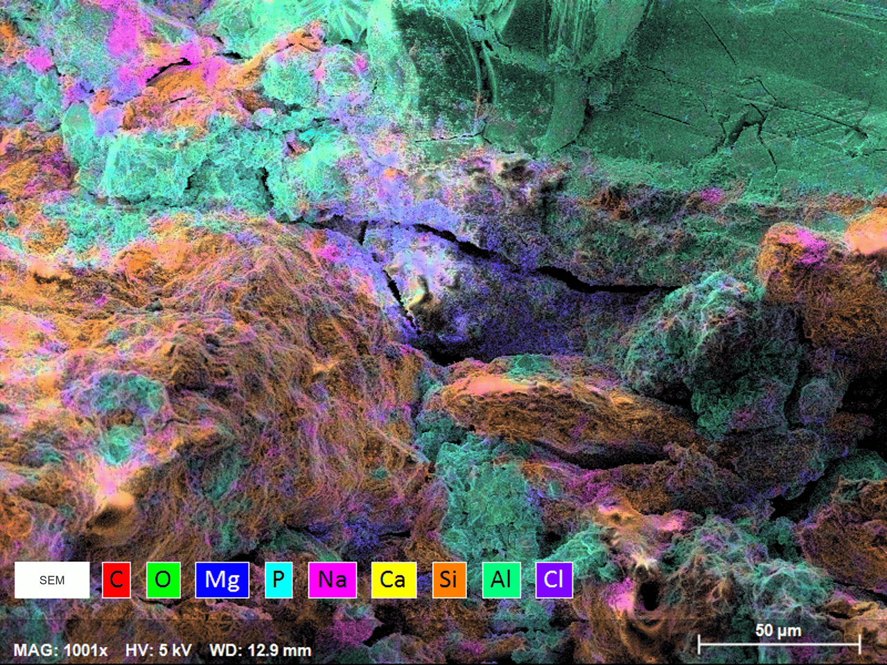
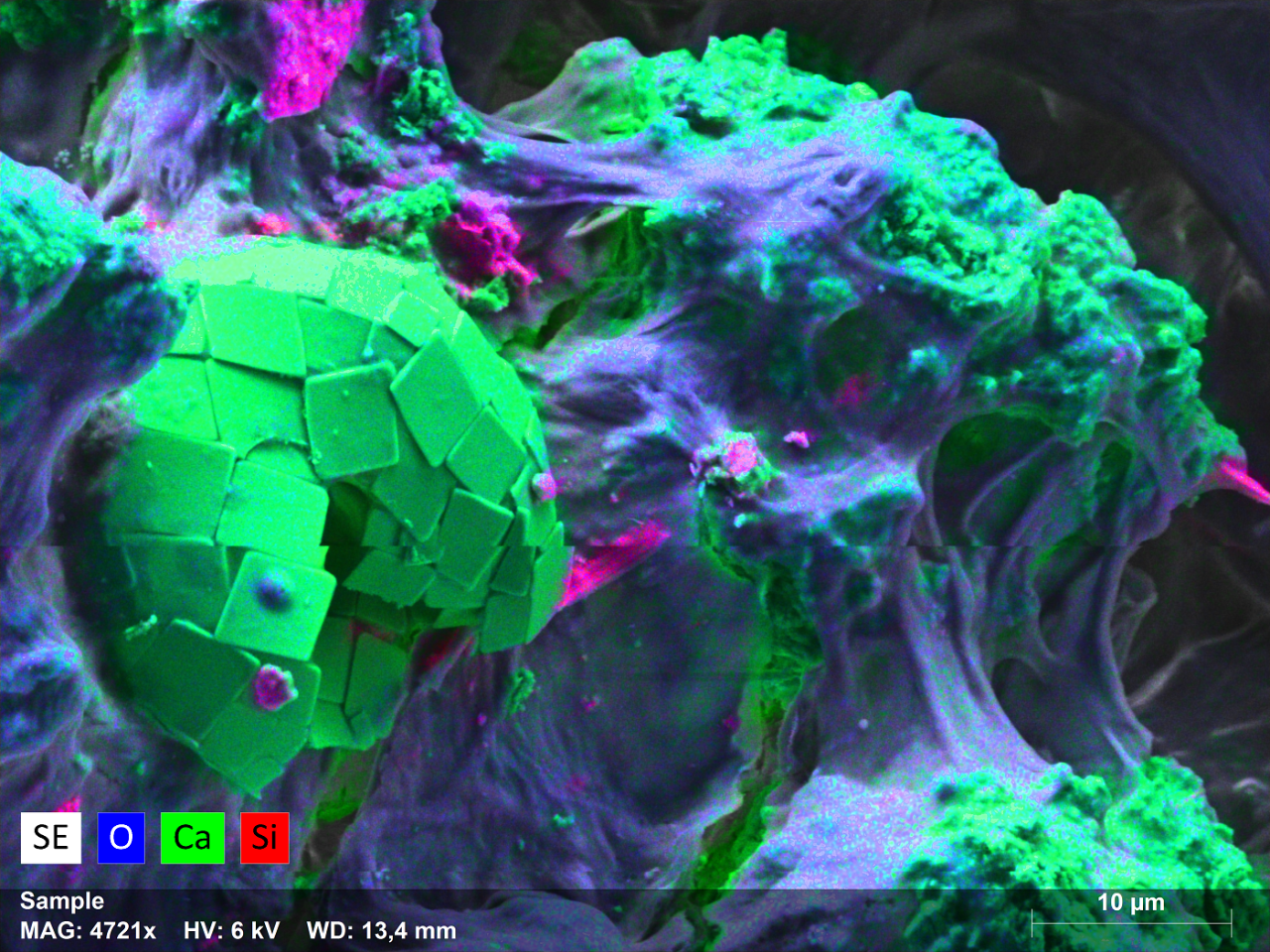
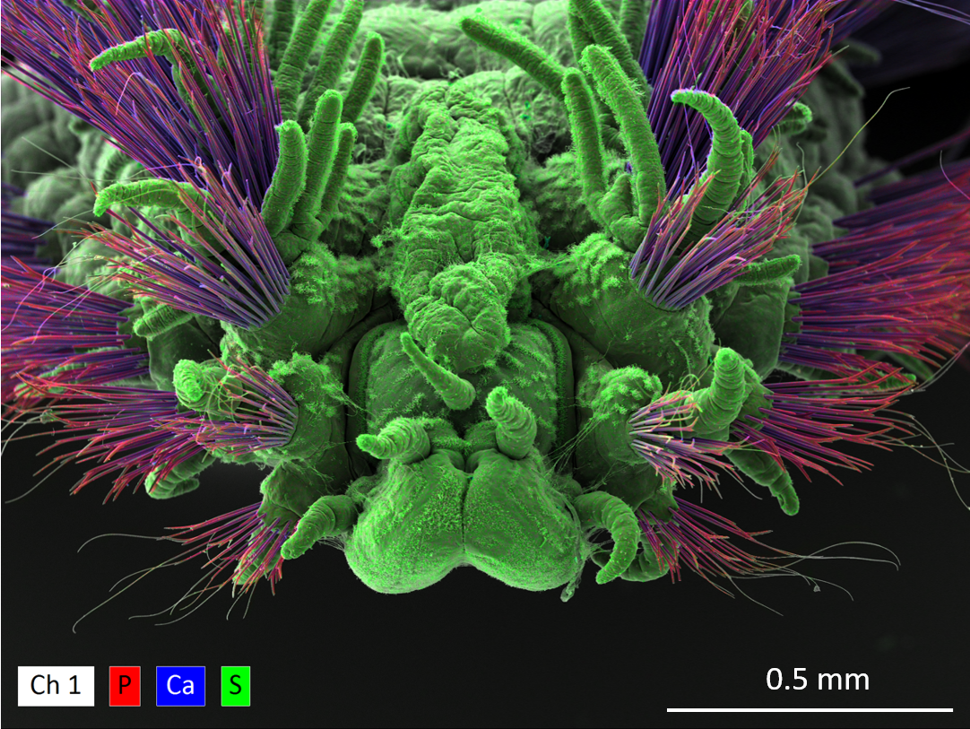
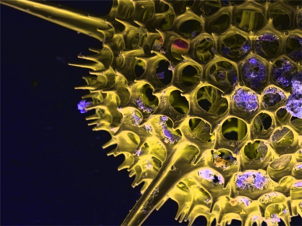
QUANTAX FlatQUAD is ideal for the elemental mapping of topographic samples with minimal shadowing effects.
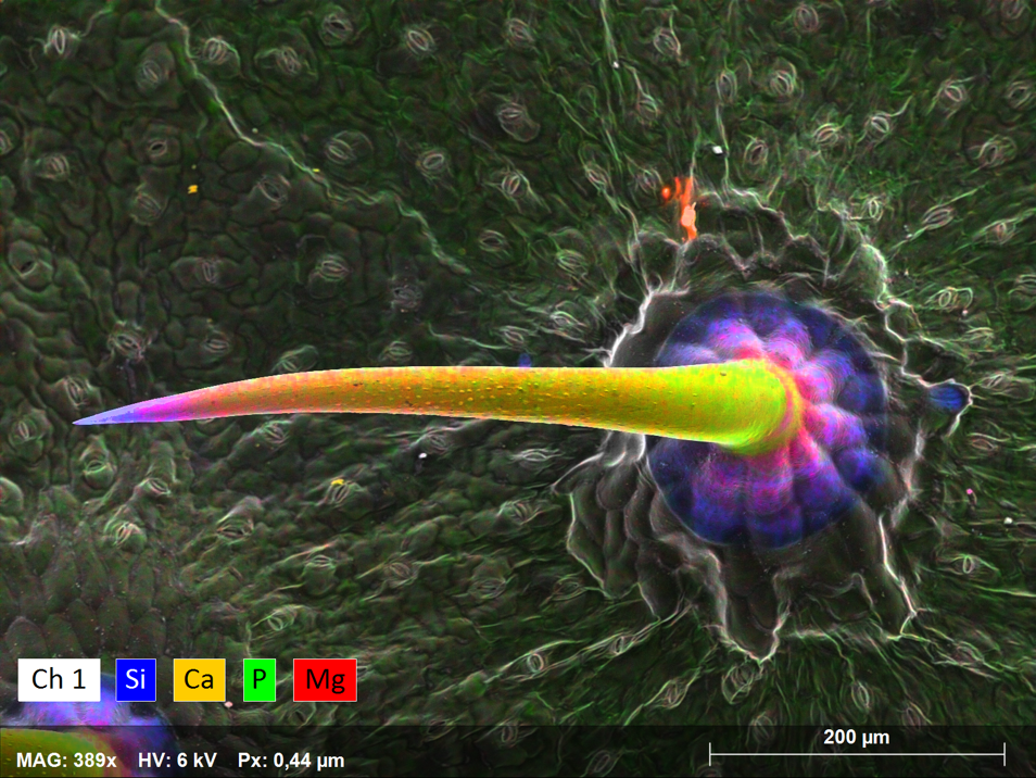
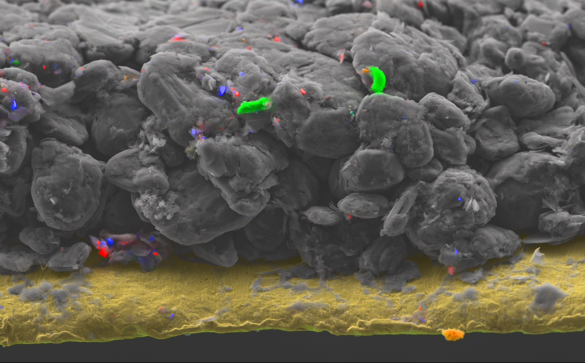
The annular design of the XFlash® FlatQUAD detector used in QUANTAX FlatQUAD provides a significantly higher takeoff angle than conventional EDS detectors. This, combined with the detector's high sensitivity allows users to analyze their samples in troughs between elevated features, allowing spectral mapping of the entire topographic specimen, and not just the easier-to-reach surfaces.
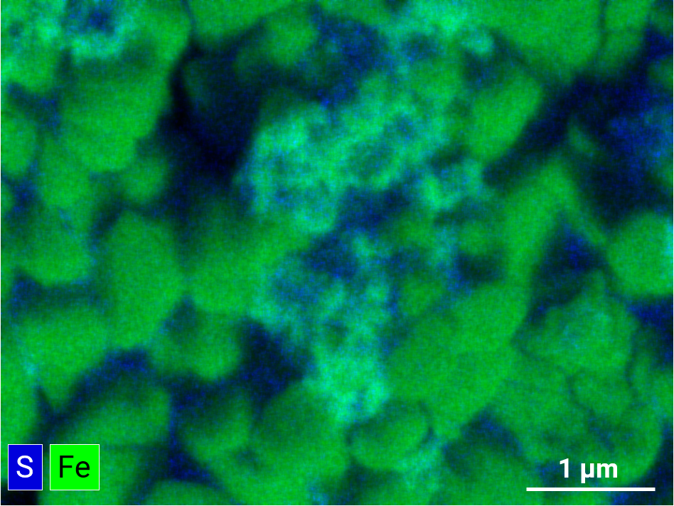
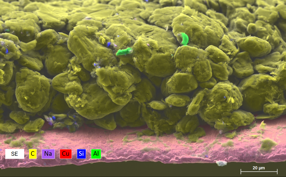
The spectral mapping of topographic samples is of particular use in the battery industry, allowing for the observation of elemental redistribution processes following charge/discharge cycles in electrode materials.

Elemental Mapping of Non-Conductive Samples
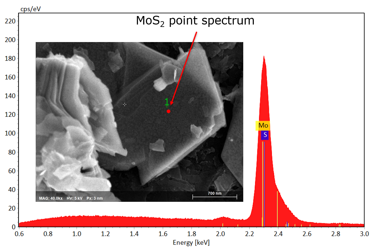
Thanks to the extremely large solid angle of the XFlash® FlatQUAD detector, QUANTAX FlatQUAD can be used to analyse samples that are difficult or even impossible to investigate using conventional systems as it can be used in the pA range:
- Non-conducting specimens can be investigated under high vacuum without carbon coating. Compared to low vacuum analysis, this approach reduces hydrocarbon contamination and avoids beam skirting effects.
- Samples with low carbon content can be analyzed, as carbon deposition caused by the electron beam is drastically reduced and result falsification avoided.
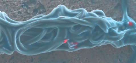
- Valuable samples (e.g., cultural heritage objects) can be analyzed in their original state without destructive sample preparation.

STEM in SEM Imaging of Electron Transparent Samples
QUANTAX FlatQUAD gives users the ability to perform STEM in SEM EDS measurements of electron transparent samples using just a SEM. This allows for high-resolution EDS without the stringent sample preparation and conditions required for a TEM.
Combined EDS with EBSD on Electron Transparent Samples
To gain even more information from your electron transparent samples, combine QUANTAX EBSD with an eWARP TKD detector.


Quantification of a Sample's Elemental Composition
Accurate elemental quantification is possible using the XFlash® FlatQUAD, allowing users to determine the elemental composition of their samples.
QUANTAX FlatQUAD is even able to quantify light elements such as boron, including at high throughput of 3,200,000 cps.

Real-Time Elemental Mapping using ESPRIT™ LiveMap
The large solid angle and high-performance parallel signal processing of the XFlash® FlatQUAD detector used in QUANTAX FlatQUAD enables live elemental mapping using the ESPRIT LiveMap feature at high count rates.
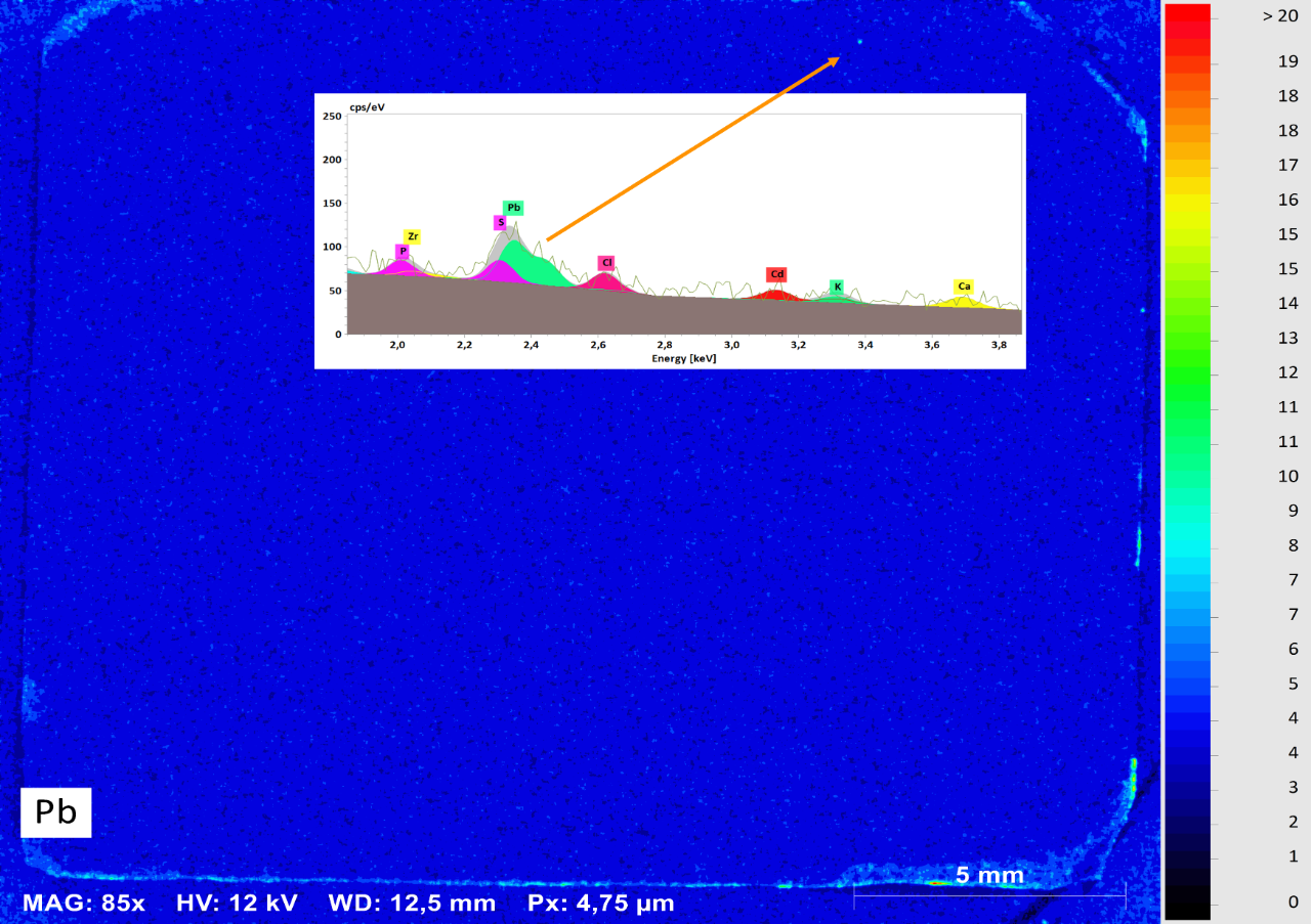
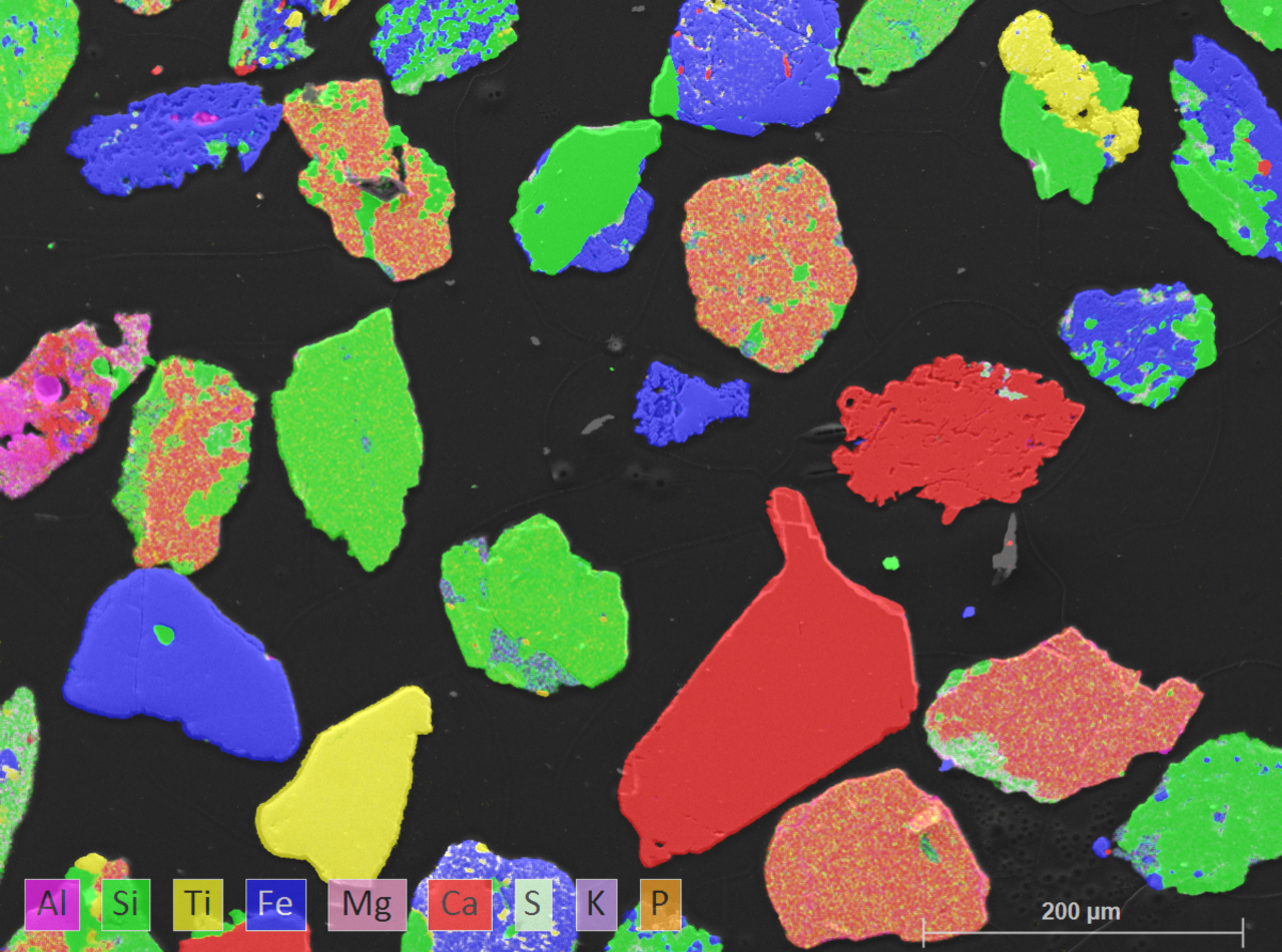
Live elemental mapping is particularly useful in preliminary sample screening. QUANTAX FlatQUAD can be used alongside ESPRIT LiveMap to identify regions of interest (ROI) within a sample – such as contamination, interfaces or localized trace elements – which can then be analyzed further and quantified using the same detector. ESPRIT LiveMap includes features such as automated element identification and peak deconvolution.
One EDS Detector for Every Task - Perform Both Qualitative & Quantitative Analysis
In addition to the unique analytical capabilities of QUANTAX FlatQUAD, which brings EDS to new application fields, it's core XFlash® FlatQUAD 2L detector also works as a standard EDS detector.
This means that both the qualitative and quantitative EDS analysis of samples is possible using just one EDS detector.
Discover Applications for QUANTAX FlatQUAD
The unique geometry of QUANTAX FlatQUAD's detector makes challenging EDS easy, opening up whole new application areas to EDS analysis.
Applications using the XFlash® FlatQUAD 2L detector:
Register Now: Step Into The Future of SEM Elemental Analysis

In this launch webinar, discover XFlash® FlatQUAD™ 2L, the first EDS detector to uniquely combine industry-leading X-ray collection efficiency with the ability to perform parallel BSE imaging.
See how co-registered elemental and contrast information can be acquired simultaneously at lower electron doses enabling faster workflows and higher spatial resolutions, even with beam-sensitive samples.
Resources
Learn more about EDS
Interested in learning more about EDS? Visit our explainer page: