半導体ソリューション
Advanced Solutions for Semiconductor
Bruker's suite of technologies for semiconductor manufacturing address critical metrology and process needs across the broadest range of applications from R&D to process improvement. 75% of the world's top 25 semiconductor manufacturers rely on Bruker metrology tools for front-end and back-end applications, including development of their next-generation products. Bruker commitment to innovation and technology leadership drives the continued release of new advancements in metrology, and has garnered numerous awards and industry recognition.
半導体向け計測ソリューション
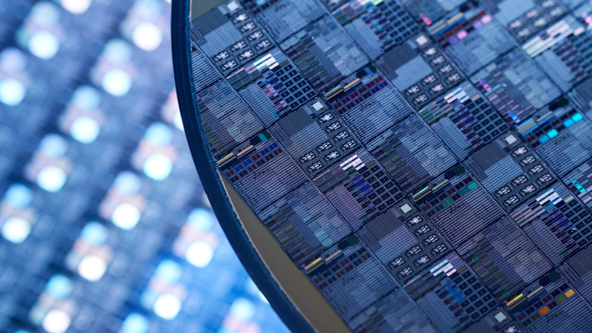
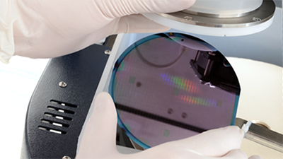
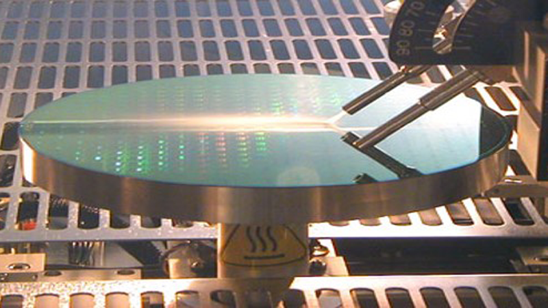
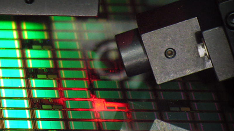
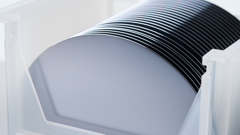
ブルカー・セミコンダクターは、新しい、高速、非接触、非破壊のX線技術をベースにする薄膜用計測ソリューションの開発、製造、販売、サポートを行っています。ブルカーは比類のないレベルの世界的な顧客サービスとサポートで知られるジョーダンバレーセミコンダクターズを買収し、その結果、世界のトップ25の半導体メーカーのうち75%が、次世代薄膜の開発を含むフロントエンドおよびバックエンド用途でブルカーの計測ツールを利用しています。ブルカーでは革新と技術のリーダーシップを維持するべく努力を続けており、計測における新たな先進技術を常に世に送り出すことで、数多くの賞を受賞し、業界での高い評価を獲得してきました。
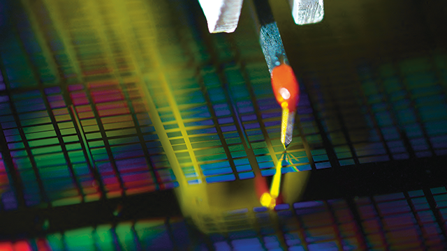
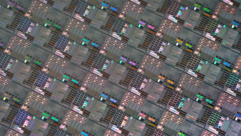
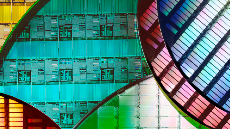
C-S薄膜素材の特性評価からウエハー基板分析、欠陥検出までのさまざまな応用分野において、ブルカーのシステムはシミュレーション解析とシミュレーションフィッティングを実現します。研究者、生産エンジニア、工程開発者が、比類のない能力を発揮できるよう、HRXRD、XRR、WA-XRD、およびXRDI測定タイプを完全にサポートしています。ブルカーは、セミファブリケーター、C-Sファブリケーター、R&Dセンター/学術研究、または工業用素材研究機関など、どのような機関であっても、お客様の計測ニーズに合った専用設計のソリューションをご用意しています。


Support

How Can We Help?
Bruker partners with our customers to solve real-world application issues. We develop next-generation technologies and help customers select the right system and accessories. This partnership continues through training and extended service, long after the tools are sold.
Our highly trained team of support engineers, application scientists and subject-matter experts are wholly dedicated to maximizing your productivity with system service and upgrades, as well as application support and training.