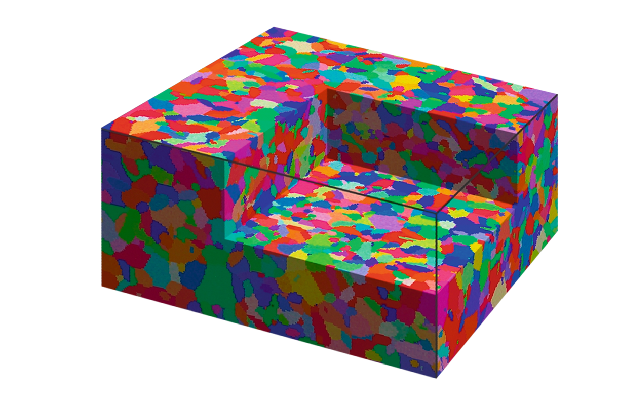
QUANTAX EBSD
With eWARP
Enter a new era of EBSD
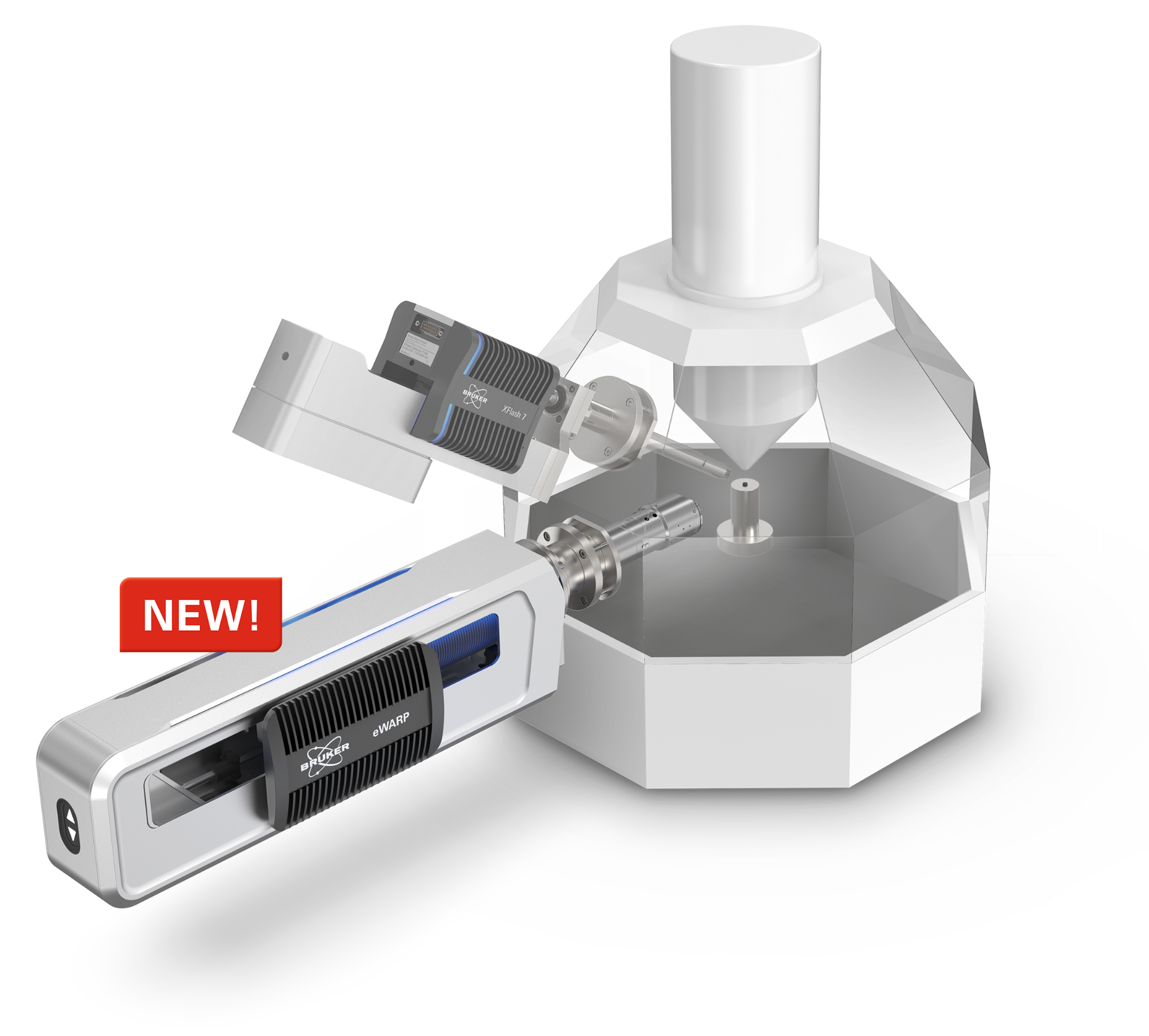
QUANTAX EBSD - Unlock the Full Potential of Electron BackScatter Diffraction
QUANTAX EBSD is a complete analytical solution for crystallographic characterization in the Scanning Electron Microscope (SEM) including EBSD detectors, EDS detectors and ESPRIT software.
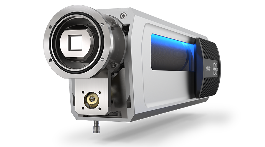
At the core of QUANTAX EBSD is our state-of-the-art eWARP detector family, powered by our award-winning WARP sensor technology, for exceptional sensitivity, speed and data quality.
From routine phase identification and grain structure analysis to the most demanding applications in advanced materials, semiconductors, energy storage, and nanoscience, QUANTAX EBSD takes you through the entire measurement process from data acquisition to analysis.
QUANTAX EBSD with eWARP: Ultra-Fast, Low kV EBSD
Enter the era of ultra-fast, low kV EBSD using QUANTAX EBSD with eWARP - the fastest and most sensitive EBSD detector ever.
Electrons Only
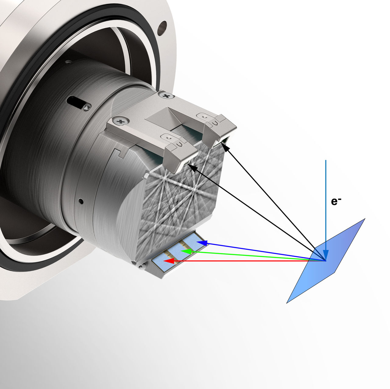
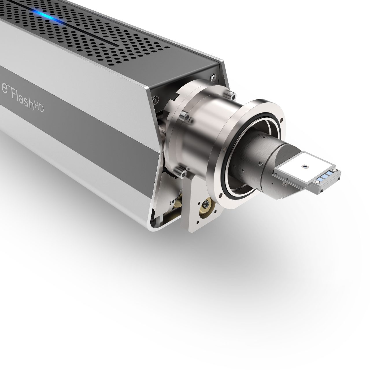
- eWARP is built with a unique WARP (Wide ARea Pixelated) hybrid pixel sensor purpose-built by Bruker specifically for EBSD.
- Extreme signal efficiency thanks to direct electron detection.
Ultra-Fast Mapping
- EBSD mapping at acquistion speeds of up to 14,400 patterns/second.
- High-resolution EBSD mapping in as little as 10 seconds.
Lightning fast FSE/BSE Imaging
- FSE/BSE imaging at acquisition speeds of up to 350,000 patterns/second
- FSE/BSE maps in just a few seconds - ideal for in-situ experiments.

QUANTAX EBSD with eWARP TKD: Unmatched TKD Performance

QUANTAX EBSD with eWARP TKD changes what is possible in nanomaterials analysis.
Accelerate Your TKD Analysis
- Acquisition speeds of up to 5,700 fps for Ultra-fast TKD.
- High-quality orientation and phase mapping within 1-5 minutes.
- Acquire maps every few seconds for in-situ analysis.
Work with Challenging Samples
- Resolutions of better than 2 nm for the analysis of complex nanostructures.
- Low-dose TKD mapping for beam-sensitive samples.
Spend Less Time Cleaning Data
- Drift correction is a thing of the past with minimal drift-induced artefacts.
QUANTAX EBSD with eWARP Detectors
QUANTAX EBSD, equipped with advanced eWARP detectors, pushes the limits of what can be achieved using EBSD.
The Fast Track to Statistically Meaningful Nanoscale Data
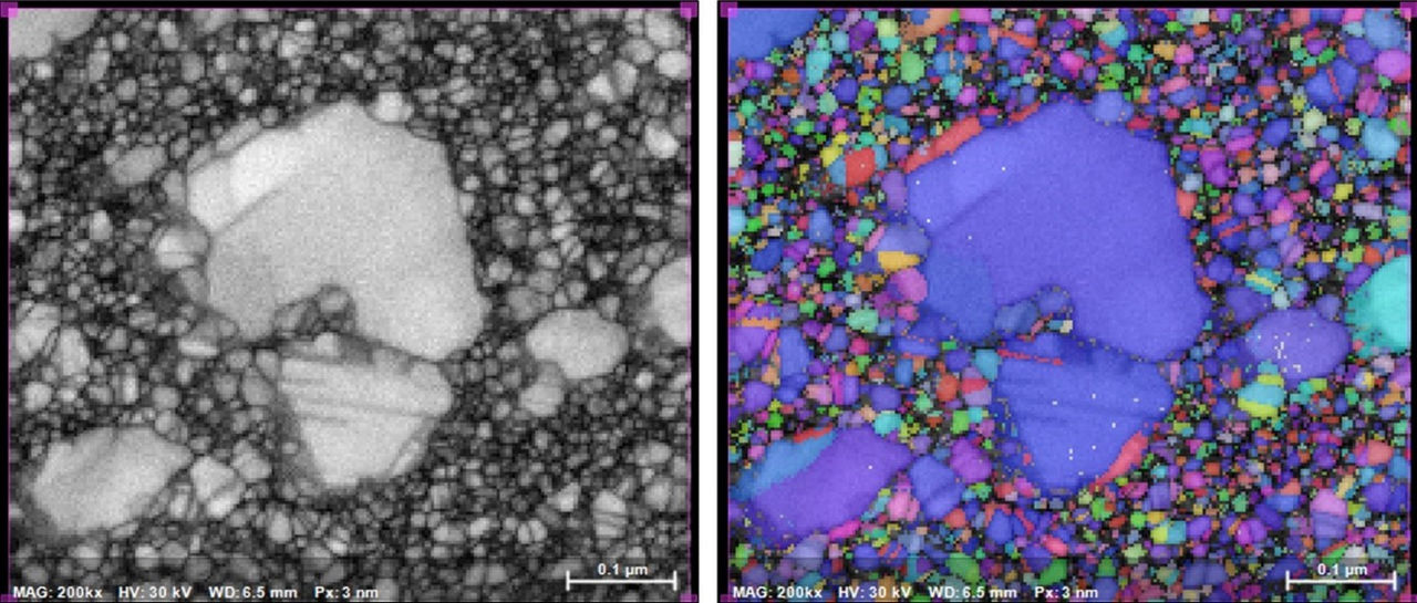
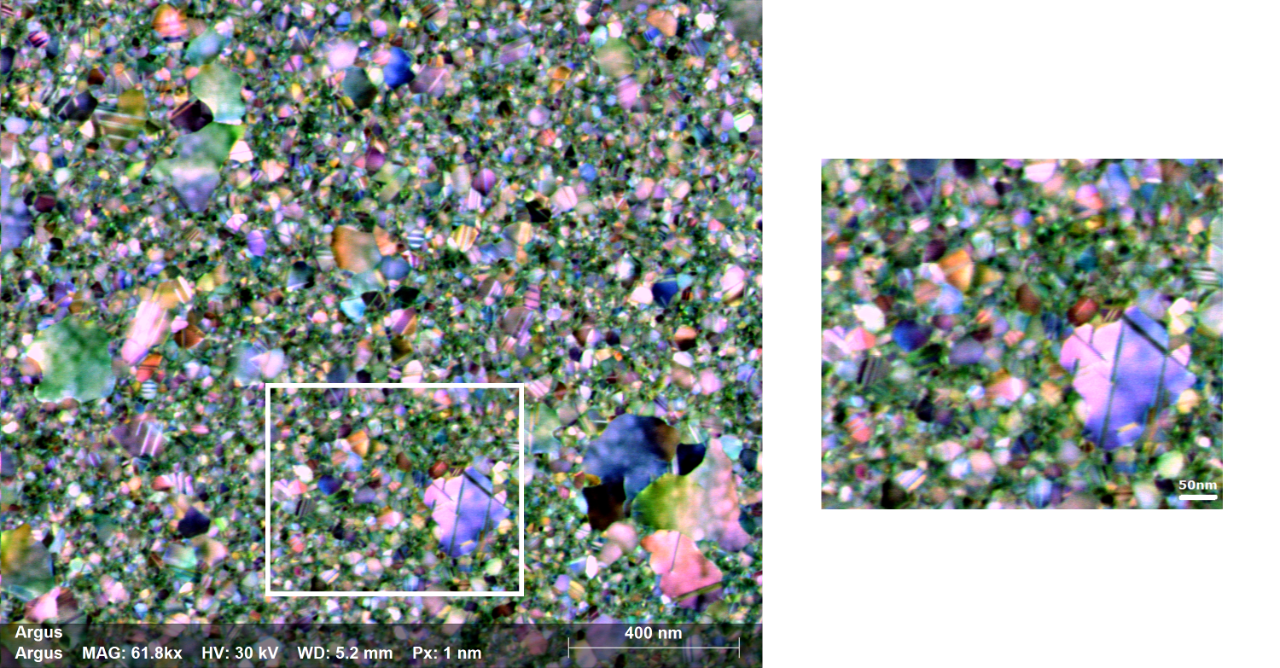
The exceptional sensitivity and speed of eWARP TKD, paired with the on-axis geometry, enable the acquisition of high-quality TKD data up to an order of magnitude faster than conventional TKD solutions while achieving sub-2 nm spatial resolution. This breakthrough in performance dramatically increases throughput for the collection of large, statistically meaningful datasets, providing greater confidence in nanoscale characterization.
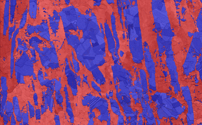
This is particularly helpful in demanding TKD applications - the TKD results shown here were acquired from an additively manufactured (AM) dual-phase steel. This analysis required the collection of large datasets over a wide area to capture a statistically significant number of Ferrite grains (red in the phase map), while simultaneously employing an ultra-fine step size to resolve the ultrafine Austenite grains (blue).
With an average indexing speed of 5,282 patterns per second, eWARP TKD combined with the ESPRIT 2 software suite acquired the entire dataset in less than 17 minutes, minimizing SEM occupancy and reducing the risk of artifacts caused by beam drift, stage drift, or sample instability. Notably, the results shown were obtained without any data cleaning or post-processing, while still achieving an indexing rate of 89.2%.


Ultra-Fast Measurements with Low Beam Requirements: High Productivity and High Resolution
eWARP requires only moderate electron beam settings, e.g. 10 kV accelerating voltage and 12 nA probe current, thanks to its unprecedented signal efficiency, even when used at its maximum speed of 14,400 patterns per second.
The patterns produced with these low beam conditions have high enough quality to be analyzed by the ESPRIT software suite with indexing rates above 99%.
In comparison with conventional EBSD maps obtained at 20 kV, the spatial resolution can be enhanced by a factor of two due to the reduced accelerating voltage. In other words, eWARP enables EBSD mapping at extreme speed with at least 25 nm resolution and excellent indexing rates.
The incredible speed and spatial resolution delivered by eWARP will have a major impact on most EBSD applications. In particular, large area mapping, 3D EBSD, and in-situ experiments will experience groundbreaking advances

Figure 2: Ni superalloy sample measured at 10 kV and 12 nA. Black frames indicate map regions in Figure 3.
Speed: 14,429 fps, Map size: 7.6 Mpixels, 84 x 56 µm2, Map time: 8:46 min, Step size: 25 nm, Indexing rate: 99%
10 kV is the New Norm: Improved Statistics and Spatial Resolution
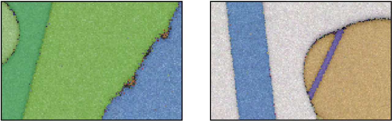
Thanks to its exceptional signal efficiency, eWARP facilitates low-kV EBSD without any disadvantages, leading to unprecedented improvements in spatial resolution and indexing quality. These innovations enable the use of EBSD as a quantitative analysis tool in previously inaccessible fields and materials.
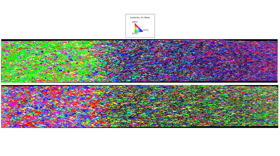
Battery materials research and production is an emerging field where EBSD demonstrates considerable potential. The grain size and the shape as well as the fraction of high-angle boundaries impact several performance factors of batteries such as capacity, charging speed, lifetime, and safety.
Figure 4 illustrates a large orientation map of a Lithium Nickel Cobalt Manganese (NCM) battery, showing the detection of even the smallest grains. The map contains around 12,000 grains. The insert in Figure 4 provides a detailed view of the fine microstructure of an NCM cathode particle.

Figure 4: Top - High-resolution EBSD map of a NCM (nickelcobalt-manganese) battery measured at 10 kV and 12 nA.
Speed: 3,300 fps, Step size: 25 nm, Map size: 3.8 Mpixels, Map time: 19:20 min
Bottom - Grain size distribution histogram corresponding to a single particle of cathode material (insert). The particle contains more than 1,000 grains with an average diameter size of 428 nm.
20 nm Resolution for Difficult Materials: Resolve Ultra-Fine Grain Materials
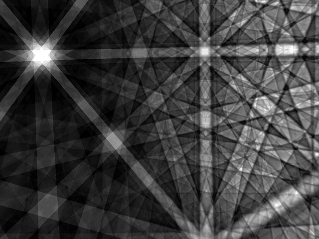
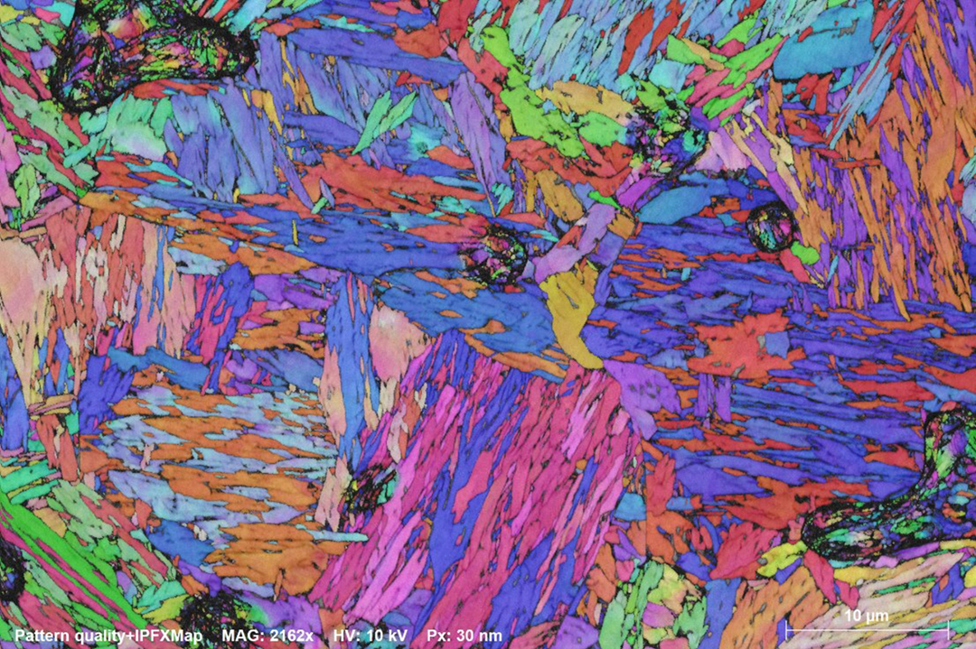
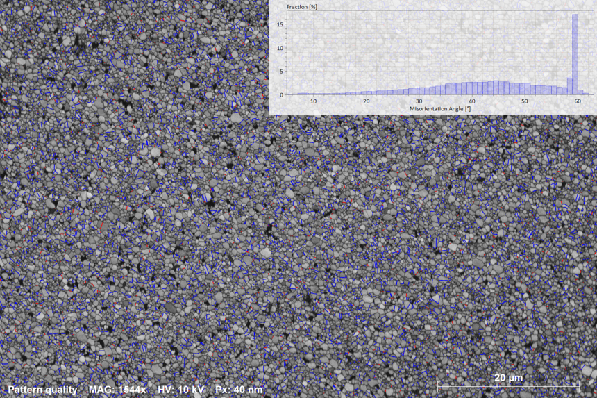
One significant advantage of 10 kV EBSD with eWARP is especially evident for the characterization of martensitic structures in steels and titanium alloys. The lower accelerating voltage minimizes the interaction volume, positively impacting both spatial resolution and the contrast in Kikuchi patterns. More visible bands result in higher probability of a correct indexing, thereby improving data quality, which is crucial for successfully correlating EBSD results with material properties.
Figure 5 presents EBSD data obtained from a martensitic stainless steel sample prepared by conventional mechanical polishing method. The pattern quality map (top) reveals a typical Martensite lath structure with a resolution of 20 nm. The corresponding crystal orientation map (bottom) clearly shows the high indexing quality in the raw data without applying data cleaning.

Fast, High-Resolution EBSD Mapping of Complex Microstructures
The exceptional sensitivity and resolution of eWARP enables detailed characterization of fine and complex microstructures.
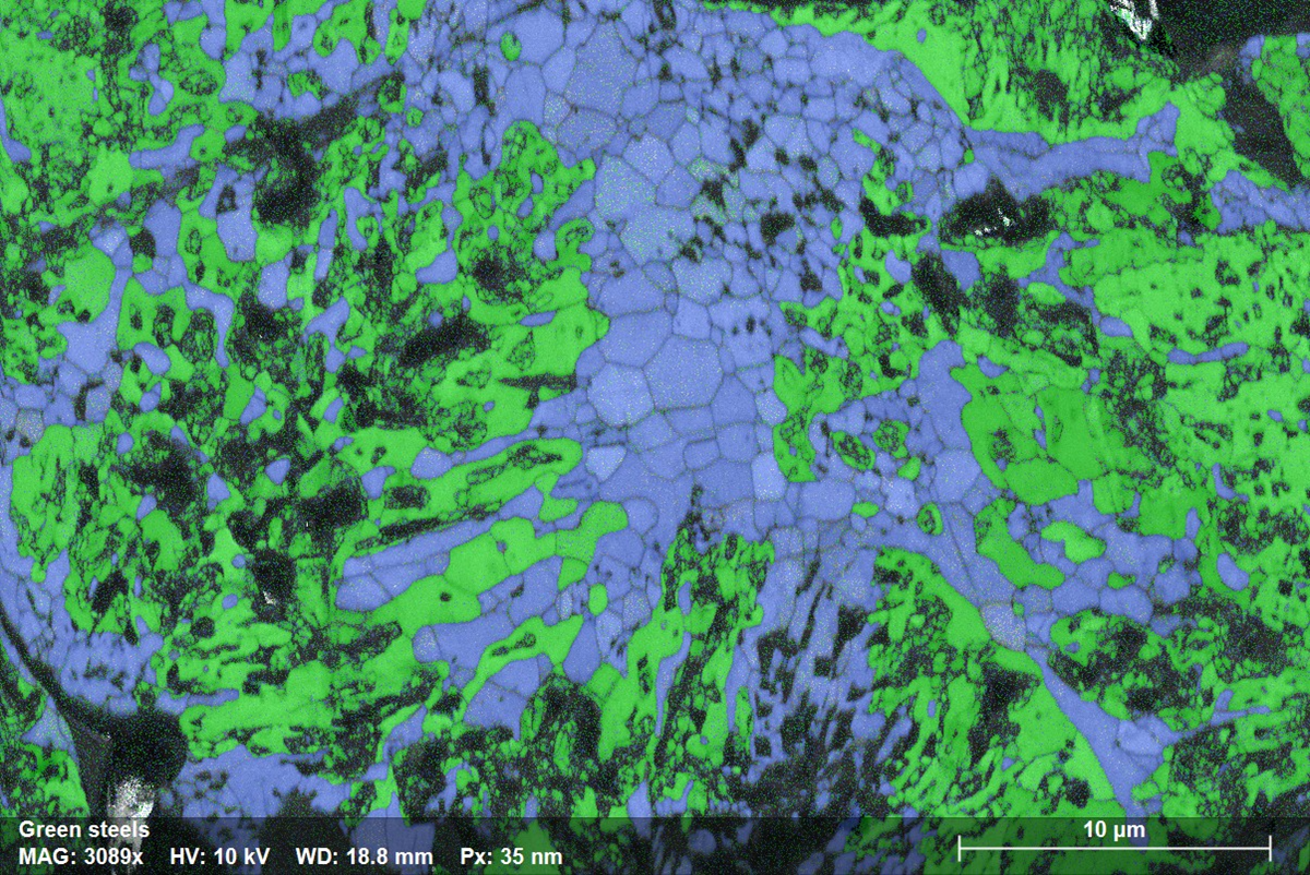
The detector's unique direct electron detection sensor allows crystallographic information to be captured from features as small as a hundred nanometers. This makes it possible to resolve intricate grain structures, sub-grain boundaries, and phase distributions.
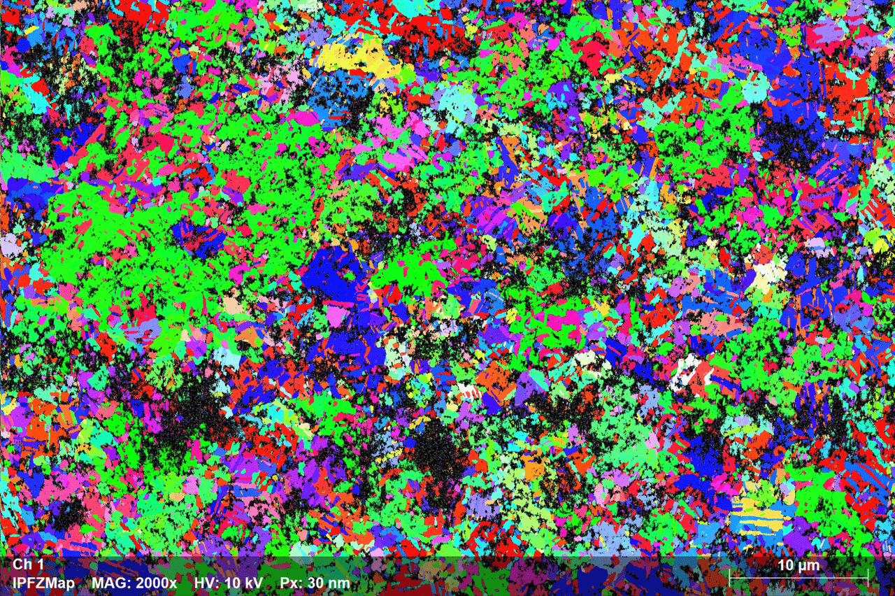
In the video example we show the EBSD mapping of a 3D-printed steel.
Augmented ARGUS™ System for FSE/BSE Imaging: Ultra-Fast, Ultra-Detailed Microanalysis
The augmented ARGUS™ imaging system provides various key features and benefits:
- Lightning-fast FSE/BSE imaging
- New virtual FSE imaging
- Orientation, topographic and phase contrast
- 1 Mpixels in just 3 seconds
- 5x images acquired simultaneously
- Color coded or grey scale
- Ideal for automated continuous acquisition during in-situ experiments
eWARP’s patented binning technology is central to the new ARGUS™ imaging system, enabling superfast FSE imaging at up to 350,000 pixels per second and providing 80 times more signal per pixel compared to native resolution mode. This results in faster and higher quality FSE images (see Figure 7).
Additionally, ESPRIT now includes the capability to create Virtual ForeScatter Electron (VFSE) images automatically during EBSD mapping, without compromising speed or signal integrity. Figure 7 shows a set of five VFSE images from a duplex stainless steel.


Figure 7: VFSE images showing orientation and topographic contrast in a duplex stainless steel sample.
Each image is created by a different area of the sensor.
ESPRIT Software - Ultra-Fast Pattern Processing, Post Processing and EDS Integration
ESPRIT is Bruker‘s intuitive software for microstructural and elemental analysis. In addition to providing the capability for in-depth EBSD analysis, ESPRIT can also integrate elemental data from EDS.

Operational Benefits: Increased Uptime and On-Site Upgrades
On-site firmware upgrades for:
- Enhanced performance
- Improved user experience
Detector monitoring for predictive maintenance (with customer permission)
On-site sensor module replacement to maximize uptime
EBSD mapping at 10 kV as the new standard – eliminating radiation damage

Applications of Electron Backscatter Diffraction Analysis
QUANTAX EBSD can be used in a wide range of microanalysis applications with the eWARP detector family for ultra-fast, low-kV EBSD as well as solutions for FSE/BSE imaging and on-axis TKD.
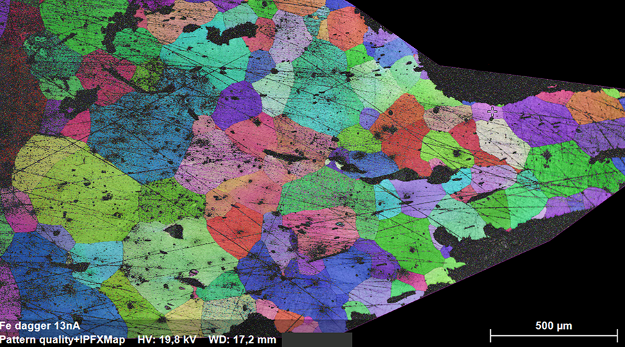
eWARP TKD - A New Frontier for Nanomaterials Research in SEM
Discover QUANTAX EBSD with eWARP TKD in this launch webinar, where we will explore the breakthrough technology behind eWARP TKD and see how it is redefining nanomaterial characterization.
Discover how exceptional signal efficiency and acquisition speeds of up to 5,700 fps enable high-quality orientation and phase maps in minutes, accelerating insights at the nanoscale.

Resources & Publications
Learn more about EBSD
Interested in learning more about EBSD? Visit our explainer page: